Ultra linear high frequency transconductor structure

a high frequency transconductor and linear technology, applied in the direction of dc-amplifiers with dc-coupled stages, amplifiers with semiconductor devices/discharge tubes, dc-amplifiers with different amplifiers, etc., can solve the problems of high power, or alternatively, low power at the expense of poor linearity

Inactive Publication Date: 2002-02-12
CONEXANT
View PDF3 Cites 31 Cited by
  • Summary
  • Abstract
  • Description
  • Claims
  • Application Information

AI Technical Summary

Problems solved by technology

Filter techniques have achieved high linearity, but at the expense of high power, or alternatively, low power at the expense of poor linearity.

Method used


Image

  • Ultra linear high frequency transconductor structure
  • Ultra linear high frequency transconductor structure
  • Ultra linear high frequency transconductor structure

Examples


Embodiment Construction

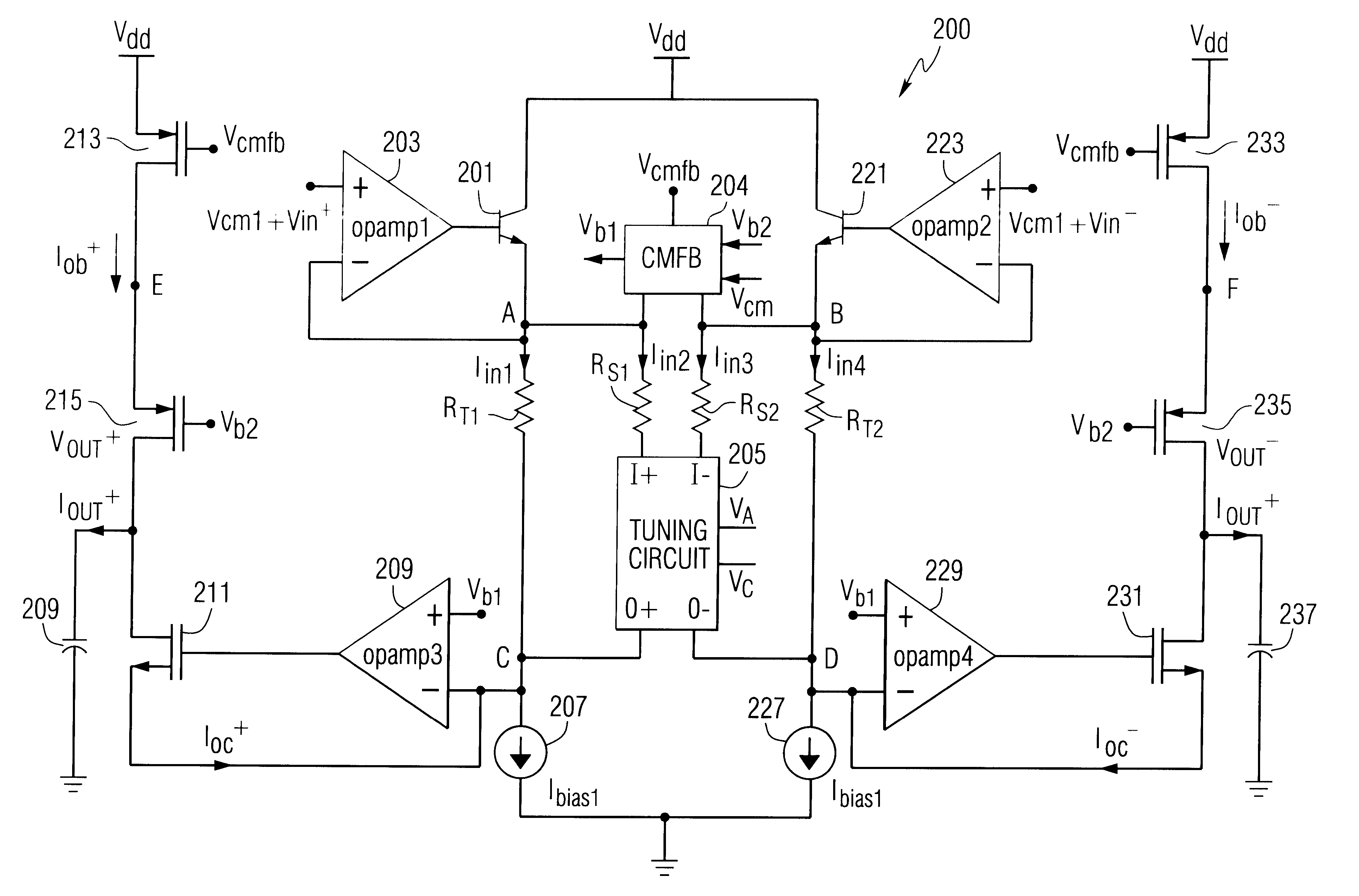
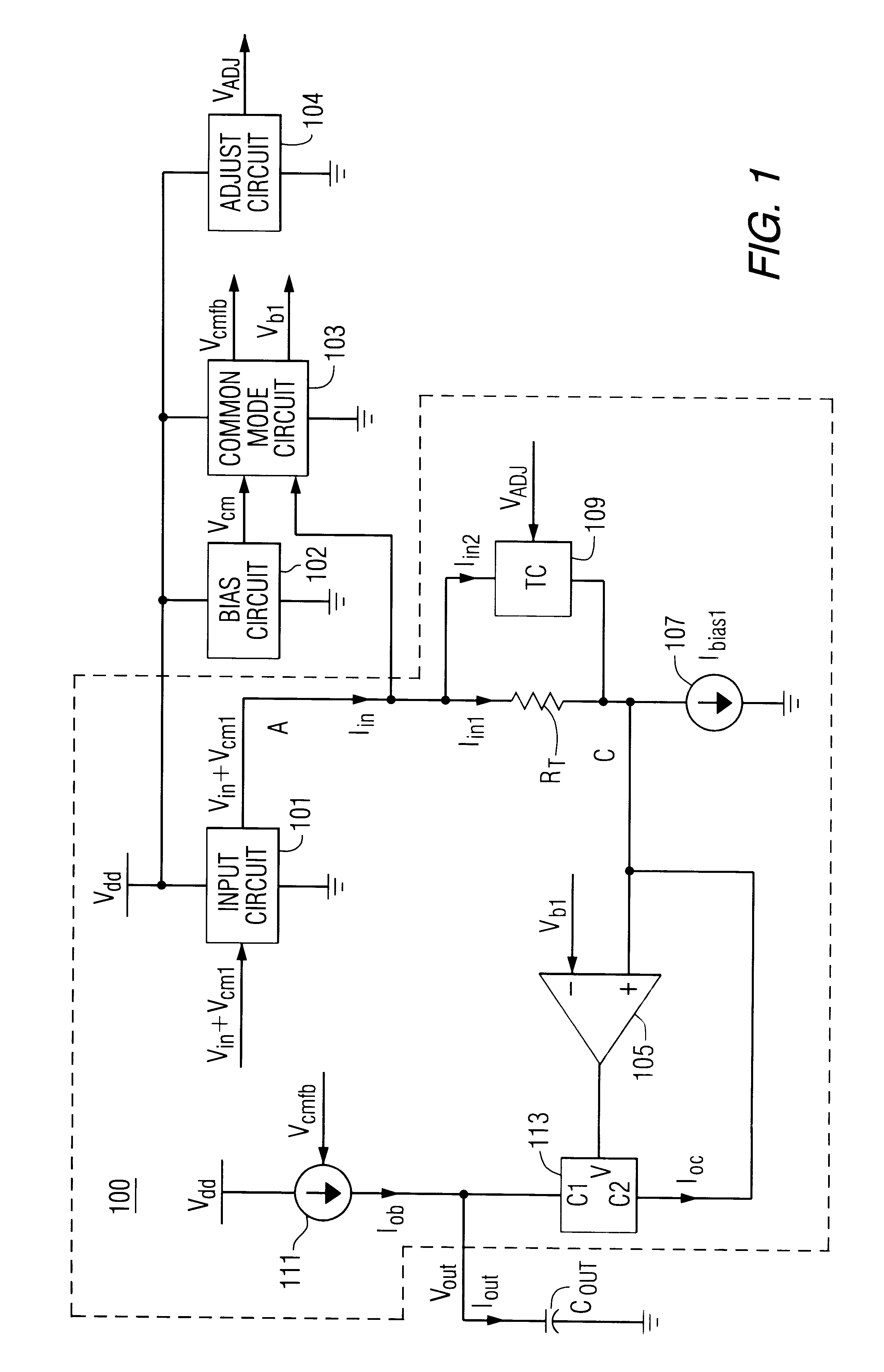
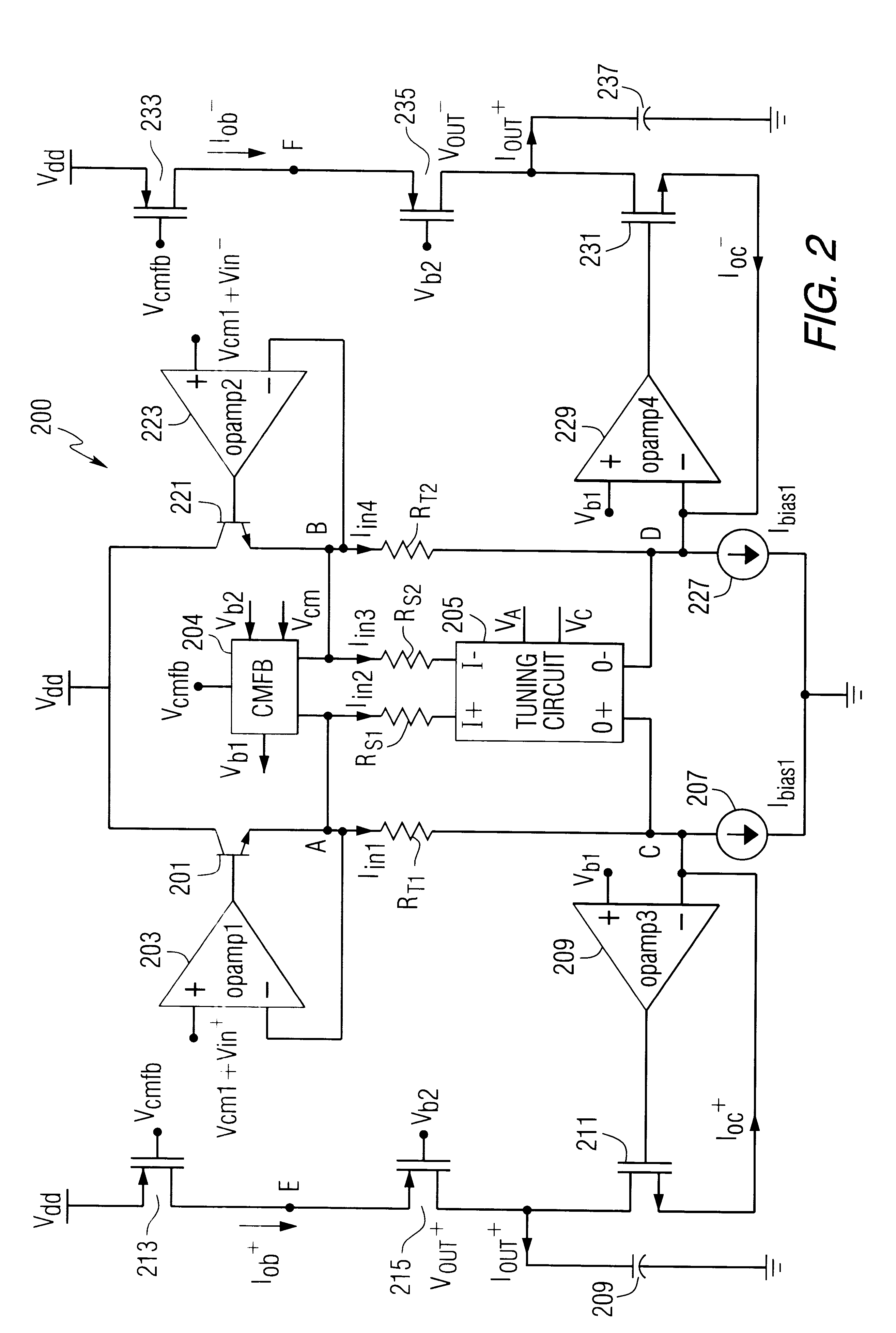
FIG. 1 is a block diagram of a simplified transconductor block 100 with capacitive load C.sub.OUT that is used to illustrate operation of a transconductor according to the present invention. The transconductor block 100 illustrates one side of a transconductor circuit, which typically receives a differential input and provides a differential output. As described further below, the transconductor block 100 may be used as a building block in which it is combined with other, similar transconductor circuits to implement amplifiers, filters, etc., as known to those skilled in the art. The transconductor block 100 is associated with and coupled to a bias circuit 102, a common mode feedback circuit (CMFB) 103 and an adjust circuit 104. The bias circuit 102, the CMFB 103 and the adjust circuit 104 may each be provided locally or globally in which each is associated with one or more transconductor blocks.

A power supply voltage, referred to as V.sub.dd, is provided to an input circuit 101 of ...


PUM


Abstract

A transconductor block including a Czarnul tuning network, transconductance resistors, an input voltage follower amplifier, a common mode circuit, PMOS transistors coupled in cascode configuration, an input current source, and high gain amplifiers that drive NMOS transistors at the output. The input voltage follower amplifier receives a differential input signal including a common mode voltage and applies the differential input signal to the Czarnul tuning network. The Czarnul tuning network includes series resistors and is coupled in parallel with the transconductance resistors. The common mode circuit receives the differential input signal and a reference common mode voltage and provides a bias voltage and a common mode feedback voltage. The common mode circuit asserts the common mode feedback voltage to the output PMOS transistors to establish a DC output current and to minimize drift of the common mode voltage of the transconductance block. Also, the bias voltage is level shifted from the common mode signal. The high gain amplifiers maintain the output of the Czarnul tuning network and transconductance resistors at the bias voltage. The high gain amplifiers are coupled to the input current sources and to the NMOS transistors in a negative feedback configuration. The high gain amplifiers drive the NMOS transistors to reflect an output current that corresponds to the input voltage signal.

Description

The present invention relates to communications, and more particularly to an ultra linear high frequency transconductor for use in communication networks.DESCRIPTION OF RELATED ARTLinearity is of utmost importance in the present day communication networks. In all wireless and wireline systems, it is very important to have low inter-channel interference and crosstalk. For example, in wireless networks it is important to maximize linearity in a channel to facilitate adapting to significant multipath propagation distortion. Linearization permits digital equalization techniques to resolve the multipath distortion.Filters are a key component in any data communication system, providing anti-alias support, channel tuning, and channel matching. Since filters are in the communication path, filter linearity is crucial. There is strong motivation to realize filters on monolithic integrated circuits to reduce external component count, and hence, to reduce the cost for the overall communication ...

Claims


Application Information

Patent Timeline
Patent Type & Authority Patents(United States)
IPC IPC(8): H03F3/45
CPCH03F3/45511H03F3/45937H03F2203/45418H03F2203/45394H03F2203/45404H03F2203/45356
Inventor MYERS, BRENT A.GANTI, RAMKISHORE
Owner CONEXANT
Why Eureka
Try Eureka