Method to control mechanical stress of copper interconnect line using post-plating copper anneal

Inactive Publication Date: 2002-04-09
GLOBALFOUNDRIES INC
View PDF12 Cites 104 Cited by
  • Summary
  • Abstract
  • Description
  • Claims
  • Application Information

AI Technical Summary

Problems solved by technology

Additionally, reducing the size, or scale, of the components of a typical transistor also increases the density, and number, of the transistors that can be produced on a given amount of wafer real estate, lowering the overall cost per transistor as well as the cost of integrated circuit devices incorporating such transistors.
Increased resistance and electromigration are undesirable for a number of reasons.
For example, increased resistance may reduce device drive current, and source/drain current through the device, and may also adversely affect the overall speed and operation of the transistor.
Additionally, electromigration effects in aluminum (Al) interconnects, where electrical currents actually carry aluminum (Al) atoms along with the current, causing them to electromigrate, may lead to degradation of the aluminum (Al) interconnects, further increased resistance, and even disconnection and/or delamination of the aluminum (Al) interconnects.
However, because aluminum (Al) has poor electromigration characteristics and high susceptibility to stress migration, it is typical to alloy aluminum (Al) with other metals.
The one criterion that is most seriously compromised by the use of aluminum (Al) for interconnects is that of conductivity.
Silver (Ag), for example, is relatively expensive and corrodes easil

Method used


Image

  • Method to control mechanical stress of copper interconnect line using post-plating copper anneal
  • Method to control mechanical stress of copper interconnect line using post-plating copper anneal
  • Method to control mechanical stress of copper interconnect line using post-plating copper anneal

Examples


Embodiment Construction

Illustrative embodiments of the invention are described below. In the interest of clarity, not all features of an actual implementation are described in this specification. It will of course be appreciated that in the development of any such actual embodiment, numerous implementation-specific decisions must be made to achieve the developers' specific goals, such as compliance with system-related and business-related constraints, which will vary from one implementation to another. Moreover, it will be appreciated that such a development effort might be complex and time-consuming, but would nevertheless be a routine undertaking for those of ordinary skill in the art having the benefit of this disclosure.

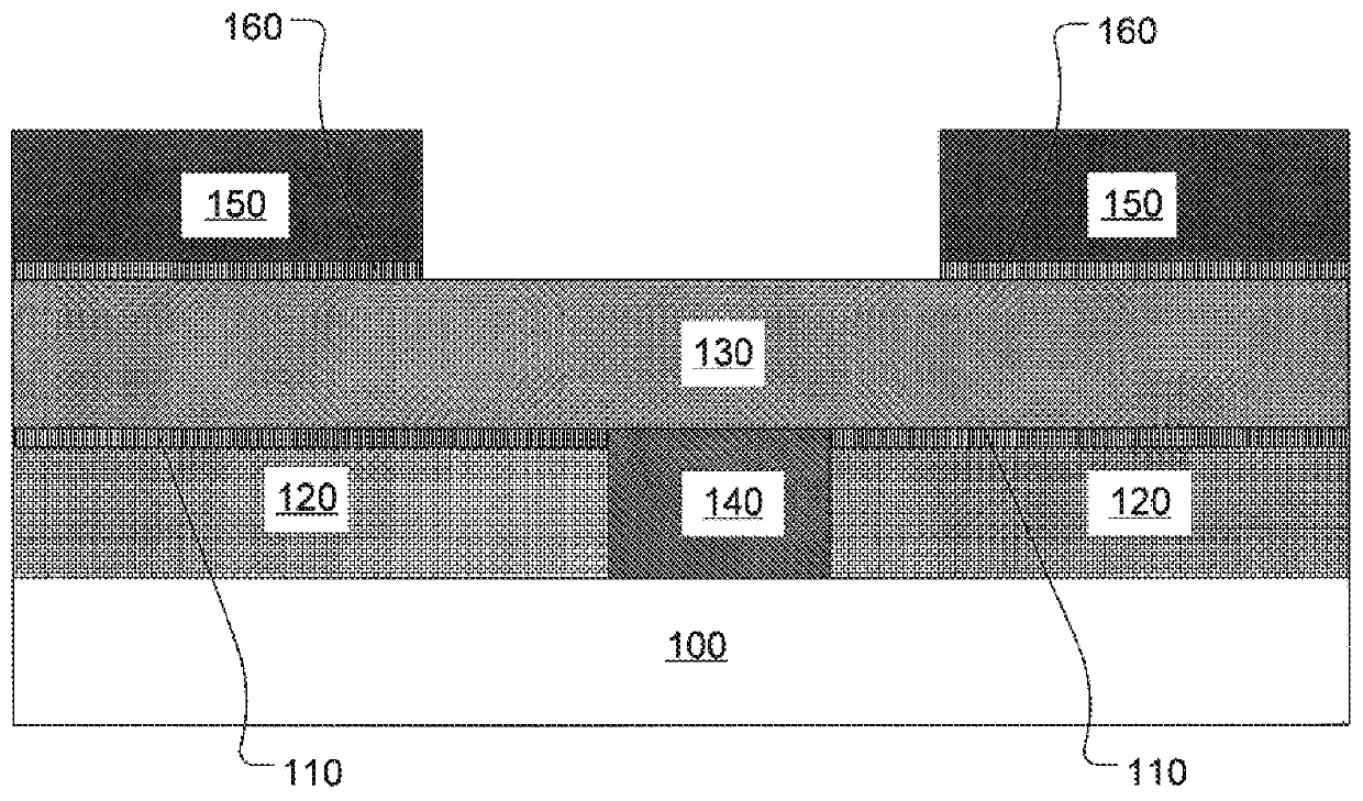
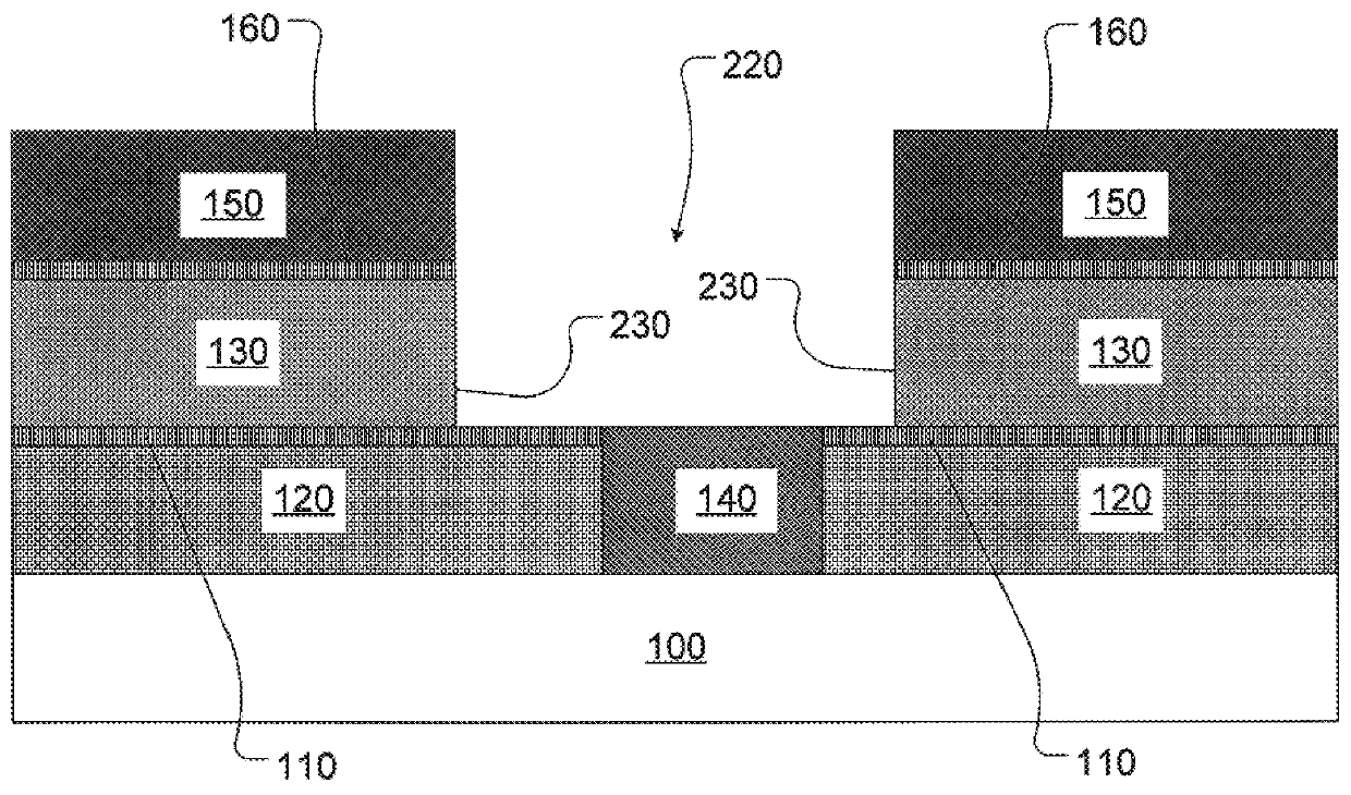
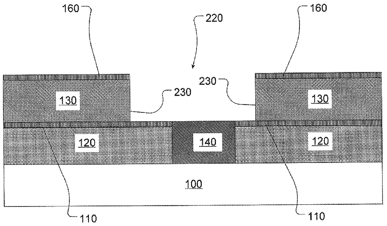
Illustrative embodiments of a method for semiconductor device fabrication according to the present invention are shown in FIGS. 1-20. Although the various regions and structures of a semiconductor device are depicted in the drawings as having very precise, sharp configurations and prof...


PUM


Abstract

A method is provided, the method comprising forming a first dielectric layer above a first structure layer, forming a first opening in the first dielectric layer, and forming a first copper structure above the first dielectric layer and in the first opening. The method also comprises annealing the first copper structure using one of a furnace anneal process performed at a temperature ranging from approximately 100-400° C. for a time ranging from approximately 10-90 minutes and a rapid thermal anneal (RTA) process performed at a temperature ranging from approximately 100-400° C. for a time ranging from approximately 10-180 seconds.

Description

1. Field of the InventionThis invention relates generally to semiconductor fabrication technology, and, more particularly, to techniques for filling contact openings and vias with copper to create copper interconnections and lines.2. Description of the Related ArtThere is a constant drive within the semiconductor industry to increase the operating speed of integrated circuit devices, e.g., microprocessors, memory devices, and the like. This drive is fueled by consumer demands for computers and electronic devices that operate at increasingly greater speeds. This demand for increased speed has resulted in a continual reduction in the size of semiconductor devices, e.g., transistors. That is, many components of a typical field effect transistor (FET), e.g., channel length, junction depths, gate dielectric thickness, and the like, are reduced. For example, all other things being equal, the smaller the channel length of the FET, the faster the transistor will operate. Thus, there is a co...

Claims


Application Information

Patent Timeline
IPC IPC(8): H01L21/70H01L21/768
CPCH01L21/7681H01L21/76877H01L21/76838
Inventor BESSER, PAUL R.
Owner GLOBALFOUNDRIES INC
Why Eureka
Try Eureka