Method of forming a photomask utilizing electron beam dosage compensation method employing dummy pattern

a lithographic method and electron beam technology, applied in the field of lithographic methods, to achieve the effect of being ready for commercialization

Inactive Publication Date: 2002-05-07
TAIWAN SEMICON MFG CO LTD
View PDF4 Cites 12 Cited by
  • Summary
  • Abstract
  • Description
  • Claims
  • Application Information

AI Technical Summary

Benefits of technology

A second object of the present invention is to provide an electron beam method in accord with the first object of the present invention wherein there is attenuated a proximity effect when exposing the blanket photoresist layer while employing the electron beam method.
A third object of the present invention is to provide a method in accord with the first object of the invention and the second object of the invention, wherein the method is readily commercially implemented.

Problems solved by technology

While direct electron beam lithographic methods are thus desirable within the art of microelectronic fabrication for forming electron beam exposed and subsequently patterned photoresist layers which are employed either directly or indirectly for forming patterned microelectronic layers within microelectronic fabrications, direct electron beam lithographic methods are nonetheless not entirely without problems in the art of microelectronic fabrication for forming electron beam exposed and subsequently patterned photoresist layers which are employed either directly or indirectly for forming patterned microelectronic layers within microelectronic fabrications.
In that regard, it is known in the art of microelectronic fabrication that electron beam exposed (directly written) and subsequently developed patterned photoresist layers are often difficult to form with uniform and anticipated linewidth resolution and fidelity encompassing various areal densities of patterned photoresist layers within microelectronic fabrications insofar as electron beam radiation when employed for directly forming patterned photoresist layers within microelectronic fabrications scatters from either within a blanket photoresist layer which is directly exposed while employing electron beam radiation (i.e., forward scattering), or in the alternative electron beam radiation also scatters from a substrate over which is formed a blanket photoresist layer which is directly exposed employing electron beam radiation (i.e., back scattering).

Method used


Image

  • Method of forming a photomask utilizing electron beam dosage compensation method employing dummy pattern
  • Method of forming a photomask utilizing electron beam dosage compensation method employing dummy pattern

Examples


Embodiment Construction

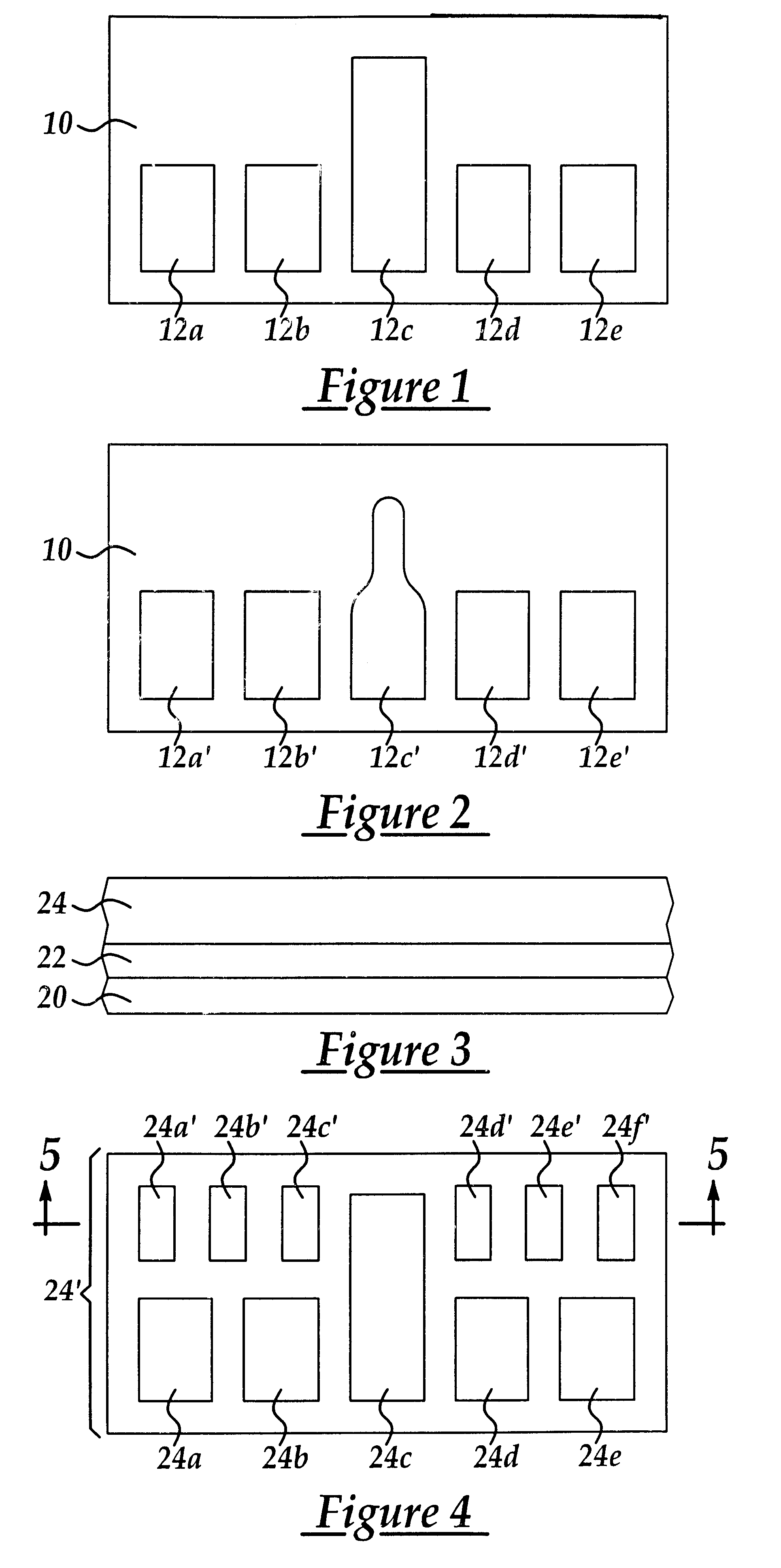
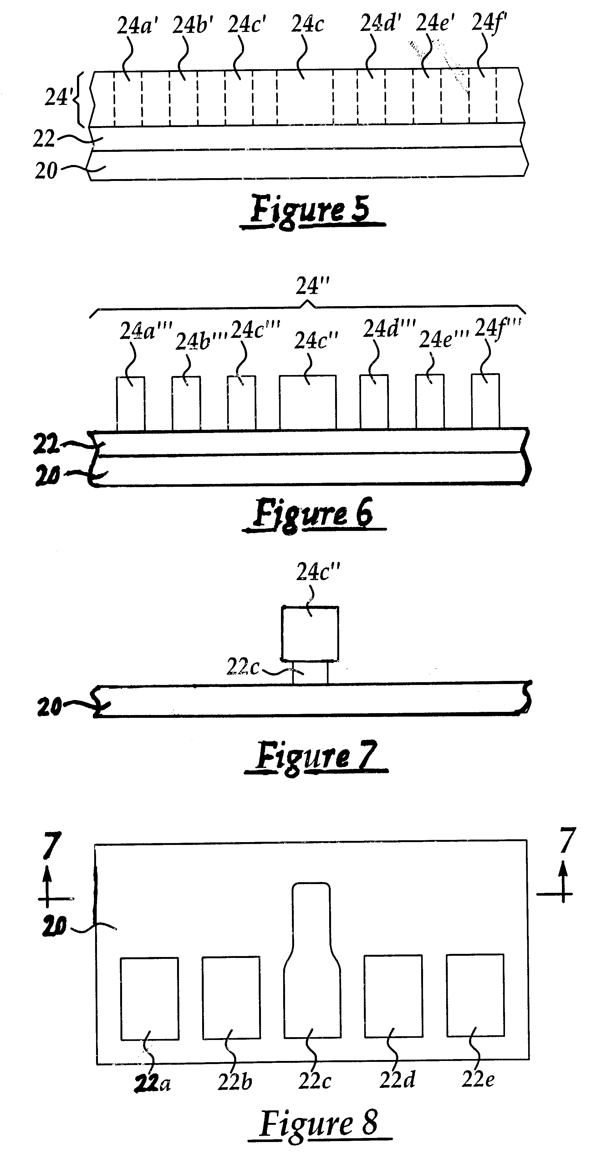
The present invention provides an electron beam method for exposing a blanket photoresist layer, where there is attenuated a proximity effect when exposing the blanket photoresist layer while employing the electron beam method. The present invention realizes the foregoing object in part by employing when exposing a blanket photoresist layer while employing an electron beam method: (1) a main latent pattern comprising a first series of latent patterns; and (2) a second (dummy) latent pattern comprising a second series of latent patterns adjacent the first series of latent patterns, wherein upon developing the main latent pattern to form a main photoresist pattern comprising a first series of patterned photoresist layers and developing the second latent pattern to form a second photoresist pattern comprising a second series of patterned photoresist layers: (1) each patterned photoresist layer within the first series of patterned photoresist layers has a first linewidth such that not a...


PUM

PropertyMeasurementUnit
thicknessaaaaaaaaaa
thicknessaaaaaaaaaa
thicknessaaaaaaaaaa

Abstract

A method for forming a patterned target layer from a blanket target layer while employing a blanket photoresist layer in conjunction with an exposure method which is susceptible to a proximity effect employs when exposing the blanket photoresist layer to form an exposed blanket photoresist layer a main latent pattern and a second latent pattern adjacent the main latent pattern. Each patterned photoresist layer formed upon developing the main latent pattern is formed of a first linewidth such that not all of a first portion of the blanket target layer formed therebeneath is etched within an isotropic etchant which is employed for etching the blanket target layer to form the patterned target layer. In contrast, each patterned photoresist layer formed upon developing the second latent pattern is formed of a second linewidth such that all of a second portion of the blanket target layer formed therebeneath is etched within the isotropic etchant which is employed for etching the blanket target layer to form the patterned target layer. The method is particularly useful for efficiently forming a photomask while attenuating a proximity effect.

Description

BACKGROUND OF THE INVENTION1. Field of the InventionThe present invention relates generally to lithographic methods employed for fabricating microelectronic fabrications. More particularly, the present invention relates to electron beam dosage compensation lithographic methods employed for fabricating microelectronic fabrications.2. Description of the Related ArtMicroelectronic fabrications are formed from microelectronic substrates over which are formed patterned microelectronic conductor layers which are separated by microelectronic dielectric layers. In the process of forming patterned microelectronic conductor layers within microelectronic fabrications, as well as in the process of forming other types of patterned microelectronic layers within microelectronic fabrications, further as well as in the process of forming patterned masking layers within photomasks which may be employed for forming patterned microelectronic layers of various varieties within microelectronic fabricatio...

Claims


Application Information

Patent Timeline
Patent Type & Authority Patents(United States)
IPC IPC(8): G03F7/20H05K3/06
CPCG03F7/2061Y10S430/143H05K3/064
Inventor WU, TSIAO-CHENTSAI, FEI-GWO
Owner TAIWAN SEMICON MFG CO LTD
Why Eureka
Try Eureka