Methods and apparatus for electropolishing metal interconnections on semiconductor devices

Inactive Publication Date: 2002-05-28
ACM RES
View PDF21 Cites 337 Cited by
  • Summary
  • Abstract
  • Description
  • Claims
  • Application Information

AI Technical Summary

Problems solved by technology

However, one potential limiting factor to developing more powerful semiconductor devices is the increasing signal delays at the interconnections (the lines of conductors, which connect elements of a single semiconductor device and/or connect any number of semiconductor devices together).
However, the closer proximity of interconnections increases the line-to-line capacitance of the interconnections, which results in greater signal delay at the interconnections.
However, this approach has the disadvantage of increasing production costs associated with forming the additional layers of metal.
Furthermore, th

Method used


Image

  • Methods and apparatus for electropolishing metal interconnections on semiconductor devices
  • Methods and apparatus for electropolishing metal interconnections on semiconductor devices
  • Methods and apparatus for electropolishing metal interconnections on semiconductor devices

Examples


Embodiment Construction

In order to provide a more thorough understanding of the present invention, the following description sets forth numerous specific details, such as specific material, parameters, and the like. It should be recognized, however, that such description is not intended as a limitation on the scope of the present invention, but is instead provided to enable a full and complete description of the exemplary embodiments.

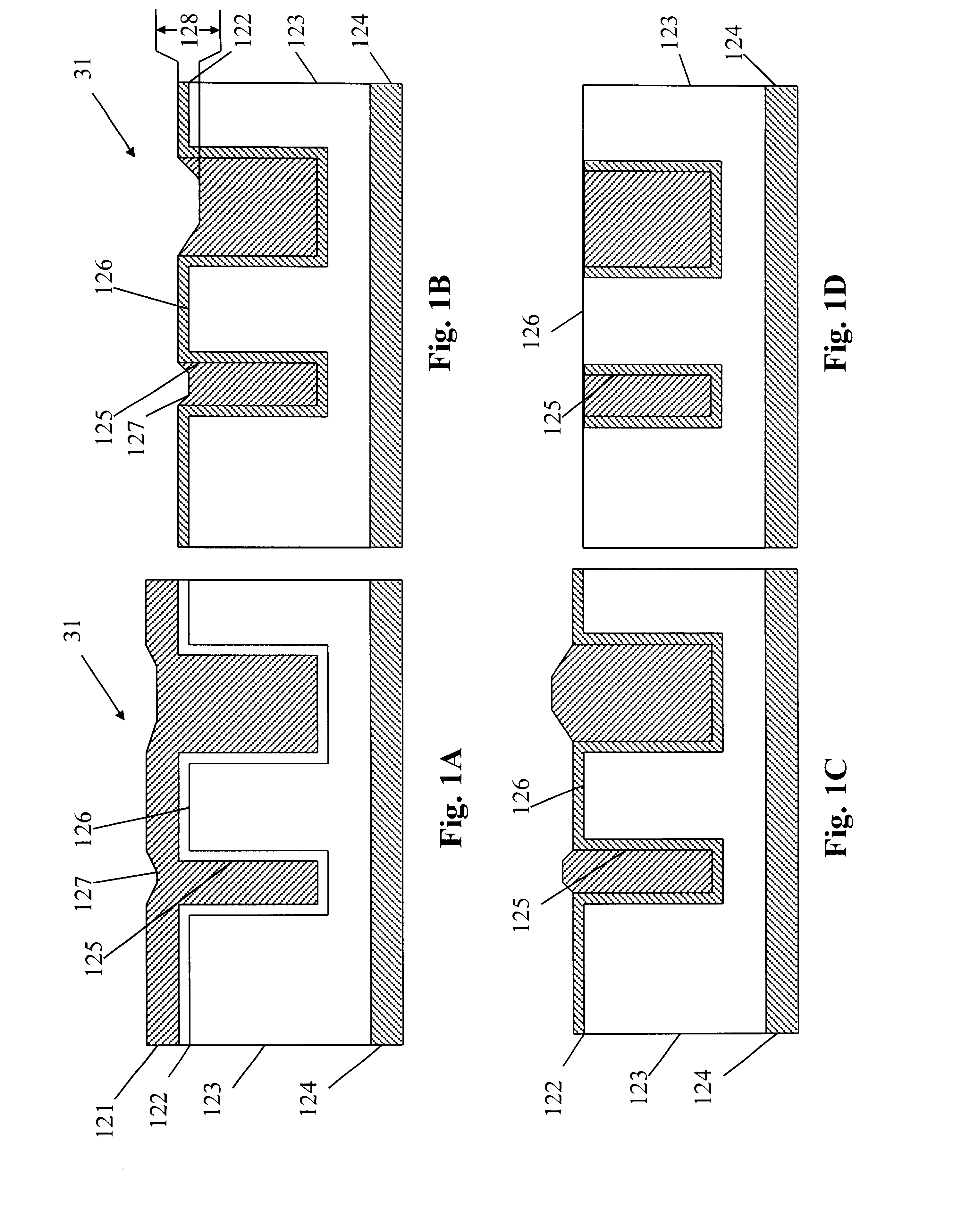
With reference to FIG. 1A, a semiconductor wafer 31, according to one aspect of the present invention, suitably includes a substrate layer 124. More particularly, in an exemplary embodiment of the present invention, substrate layer 124 preferably includes silicon. It should be recognized, however, that substrate layer 124 can include various semiconductor materials, such as gallium arsenide and the like, depending on the particular application.

Semiconductor wafer 31, according to another aspect of the present invention, suitably includes a dielectric layer 123 formed on top o...


PUM

PropertyMeasurementUnit
Temperatureaaaaaaaaaa
Fractionaaaaaaaaaa

Abstract

An electropolishing apparatus for polishing a metal layer formed on a wafer (31) includes an electrolyte (34), a polishing receptacle (100), a wafer chuck (29), a fluid inlet (5, 7, 9), and at least one cathode (1, 2, 3). The wafer chuck (29) holds and positions the wafer (31) within the polishing receptacle (100). The electrolyte (34) is delivered through the fluid inlet (5, 7, 9) into the polishing receptacle (100). The cathode (1, 2, 3) then applies an electropolishing current to the electrolyte to electropolish the wafer (31). In accordance with one aspect of the present invention, discrete portions of the wafer (31) can be electropolished to enhance the uniformity of the electropolished wafer.

Description

1. Field of the InventionThe present invention generally relates to methods and apparatus for electropolishing metal layers on semiconductor wafers. More particularly, the present invention relates to a system for electropolishing interconnections in semiconductor devices formed on semiconductor wafers.2. Description of the Related ArtIn general, semiconductor devices are manufactured or fabricated on disks of semiconducting materials called wafers or slices. More particularly, wafers are initially sliced from a silicon ingot. The wafers then undergo multiple masking, etching, and deposition processes to form the electronic circuitry of semiconductor devices.During the past decades, the semiconductor industry has increased the power of semiconductor devices in accordance with Moore's law, which predicts that the power of semiconductor devices will double every 18 months. This increase in the power of semiconductor devices has been achieved in part by decreasing the feature size (i.e...

Claims


Application Information

Patent Timeline
IPC IPC(8): C25F3/22C25F3/00C25F7/00H01L21/02H01L21/321H01L21/768H01L21/70H01L21/3213B23H5/08H01L21/304H01L21/3205
CPCC25F3/22C25F7/00H01L21/32115H01L21/7684H01L21/32134H01L21/3063
Inventor WANG, HUI
Owner ACM RES
Why Eureka
Try Eureka