
Process and apparatus for producing a laminate for electronic parts

Inactive Publication Date: 2002-08-06
TEIJIN LTD
View PDF14 Cites 12 Cited by
  • Summary
  • Abstract
  • Description
  • Claims
  • Application Information

AI Technical Summary

Benefits of technology

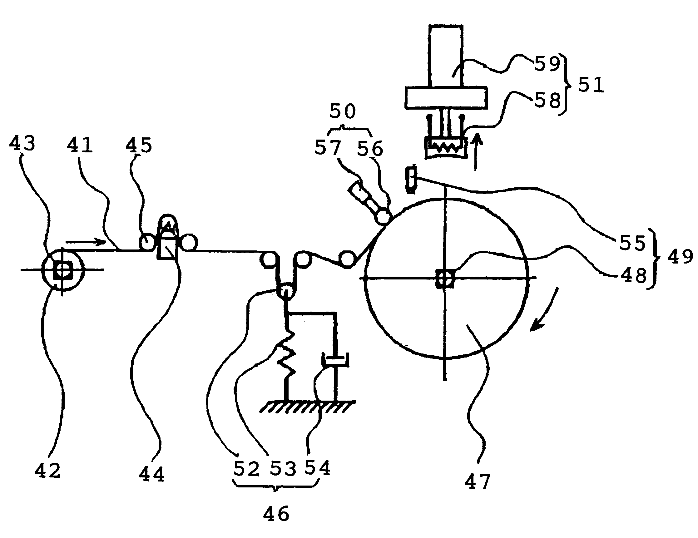
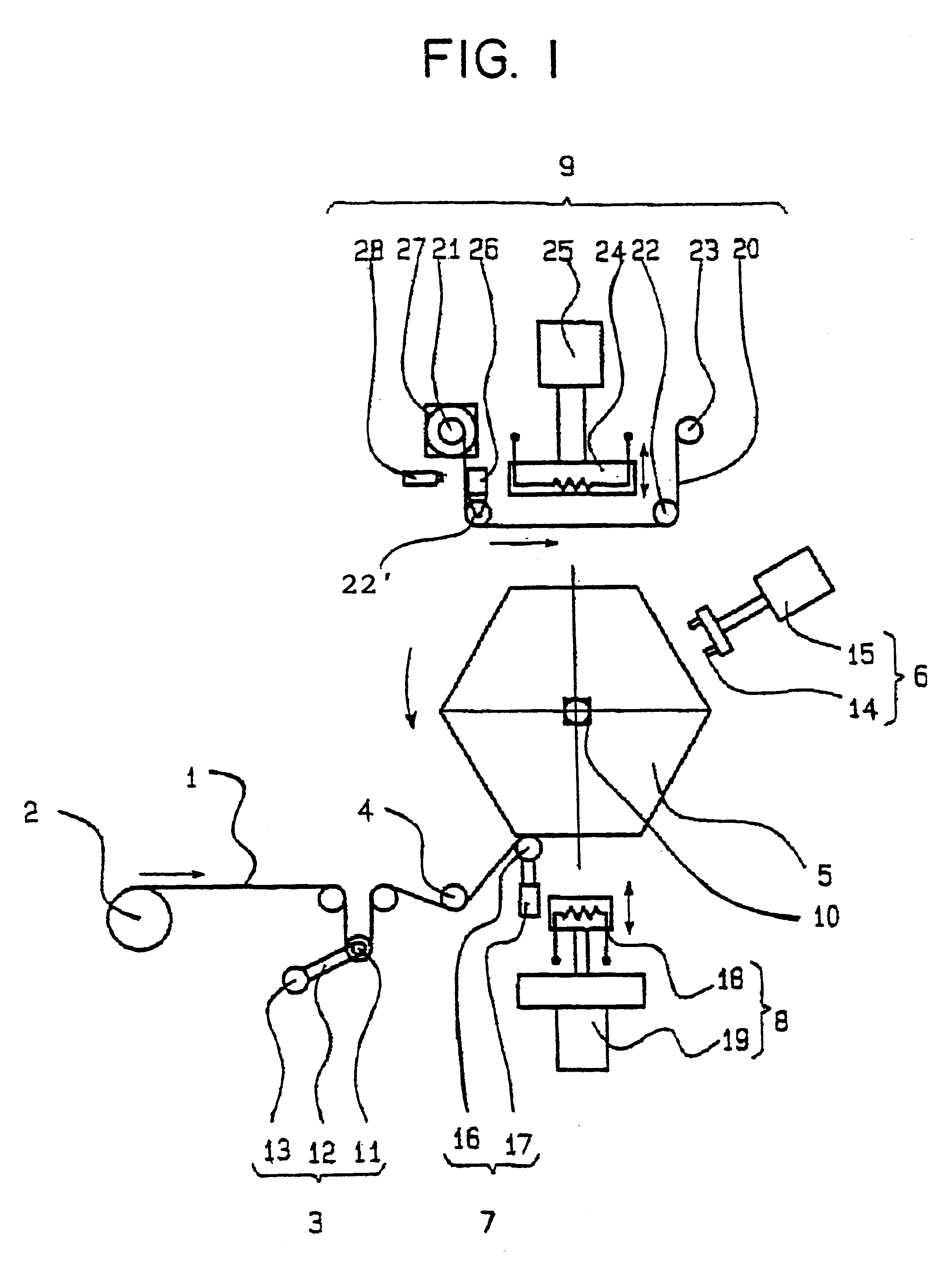
It is another object of the present invention to provide an apparatus capable of producing a multi-layer laminate for electronic parts using a self-supporting green sheet containing inorganic powder and an organic binder with a high output on an industrial scale.
It is still another object of the present invention to provide a process for producing a laminate for electronic parts such as a ceramic capacitor, particularly a multi-layer laminate, industrially advantageous.
the step of thermally relaxing the obtained laminate wound round the columnar roll to control shrinkage in the lamination plane at 200.degree. C. to 1% or less; and

Problems solved by technology

However, in an apparatus for producing a laminate electronic part by laminating together a plurality of ceramic green sheets as described above, an increase in the number of ceramic green sheets for a reduction in the thickness and an increase in the number of layers of a ceramic laminate requires a lot of time for the production of a single laminate.
This publication discloses a multi-layer magnetic capacitor as an example of this unprocessed compressed material but does not teach a process and an apparatus for producing the same.

Method used


Image

  • Process and apparatus for producing a laminate for electronic parts
  • Process and apparatus for producing a laminate for electronic parts
  • Process and apparatus for producing a laminate for electronic parts

Examples


example 2

An electrode pattern was formed on a 12 cm-wide, 14 .mu.m-thick green sheet comprising 91 wt % of a ceramic essentially composed of barium titanate and 9 wt % of ultra high molecular weight polyethylene and having a porosity of 20%. The pattern consisting of 6.92 mm.times.1.3 mm quadrilaterals was formed on the green sheet using a silver / palladium conductive paste (70 / 30) by a screen printing. The long axis of the pattern was parallel to a longitudinal direction of the green sheet, and the quadrilaterals of the pattern were arranged in 30 rows in a transverse direction of the green sheet at intervals of 0.6 mm.

Two of the green sheet (G1, G2) were wound round a cylindrical bobbin having a circumference of 1,196 mm together in such a manner that the green sheet G2 was placed upon the green sheet G1. After portions having no pattern printed thereon of the two green sheets were first wound round the cylindrical bobbin seven times, portions having a pattern printed thereon of the two gre...

example 3

An electrode rectangular pattern was formed on a 12 cm-wide, 20 .mu.m-thick green sheet comprising 91 wt % of a ceramic essentially composed of barium titanate and 9 wt % of ultra high molecular weight polyethylene and having a porosity of 10%. The pattern consisting of 6.92 mm.times.1.3 mm quadrilaterals was formed on the green sheet by a screen printing using a silver / palladium conductive paste (70 / 30). The long axis of the pattern was parallel to the edge of the green sheet, and the quadrilaterals of the pattern were arranged in 30 rows in a transverse direction at intervals of 0.6 mm.

The green sheet was wound round a cylindrical bobbin having a circumference of 1,200 mm. A portion having no pattern printed thereon of the green sheet was first wound round the cylindrical bobbin 15 times and then another portion having a pattern printed thereon of the green sheet was wound in such a manner that the pattern of a first layer was spaced apart from the pattern of a second layer by hal...


PUM

PropertyMeasurementUnit
Fractionaaaaaaaaaa
Angleaaaaaaaaaa
Percent by volumeaaaaaaaaaa

Abstract

An apparatus and a process for producing a laminate for electronic parts such as ceramic capacitors. After a predetermined pattern for forming an internal conductive layer is formed on a self-supporting green sheet which contains inorganic powder and an organic binder, the self-supporting green sheet is taken up by a columnar roll and laminated. At this point, the position of the same pattern on the green sheet G2 of the next cycle to be laminated adjacently onto the green sheet G1 of the previous cycle as the above pattern with respect to the predetermined pattern on the green sheet G1 taken up by the columnar roll is determined.

Description

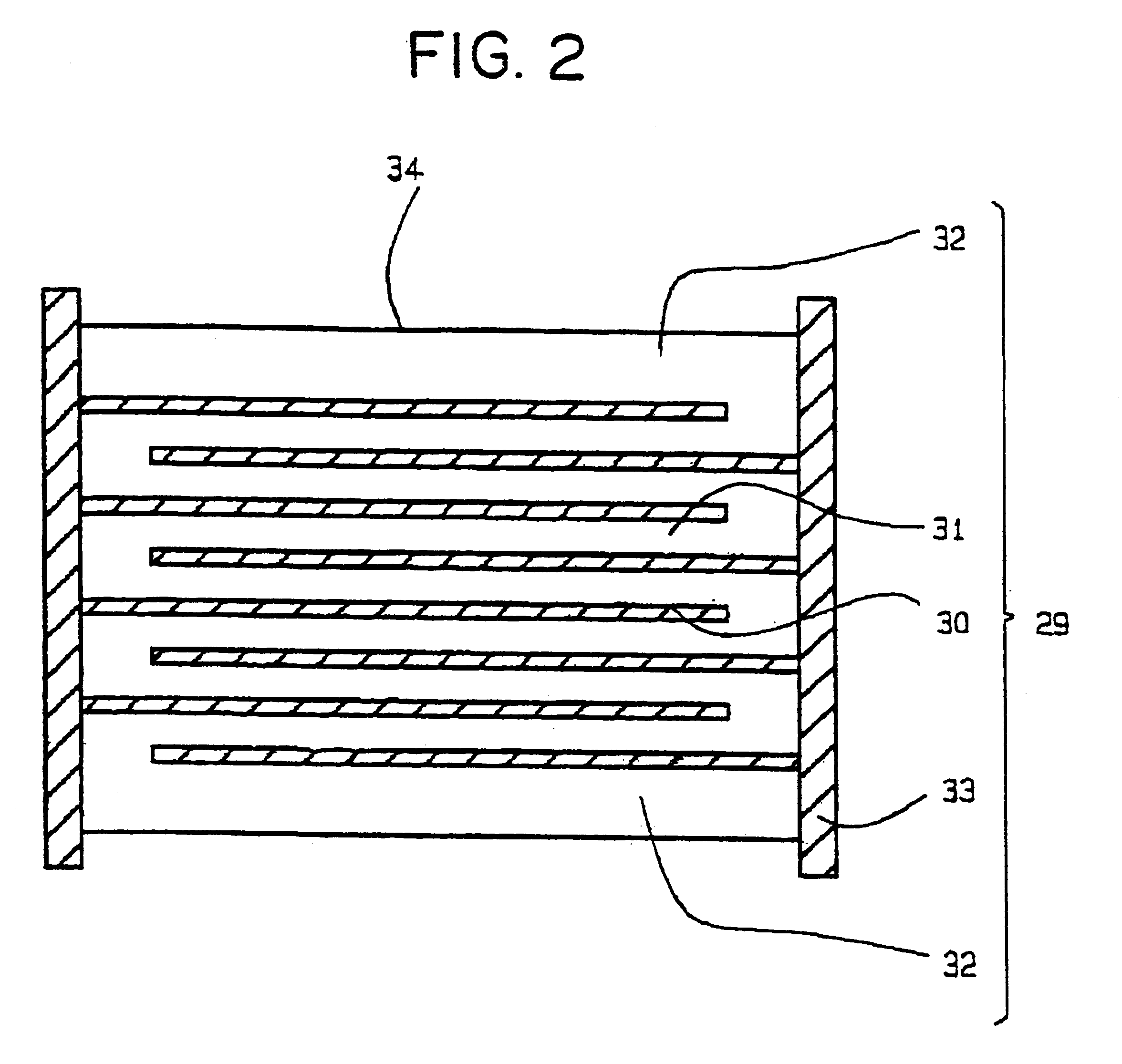
The present invention relates to a process and an apparatus for producing a laminate for electronic parts such as ceramic capacitors. More specifically, it relates to a process and an apparatus capable of producing a multi-layer laminate for electronic parts with a high output on an industrial scale.PRIOR ARTIn recent years, in the field of electronic parts, along with a tendency toward high-density surface mounting, it has been desired to reduce the sizes of laminate electronic parts such as laminate ceramic capacitors, laminate varistors, laminate filters and laminate piezoelectric elements and to improve the functions of these laminate electronic parts. A laminate ceramic capacitor is taken as an example hereinafter.A laminate ceramic capacitor comprises a plurality of dielectric ceramic layers, a plurality of internal electrodes formed between respective adjacent ceramic layers and external electrodes connected to the respective internal electrodes at the ends of the dielectric ...

Claims


Application Information

Patent Timeline
IPC IPC(8): H01G4/30H05K3/46H05K1/03
CPCH01G4/30H05K1/0306Y10T29/435H05K3/4638Y10T156/1052H05K3/4629
Inventor OHNO, TAKAOKIDO, NOBUAKINAKAMURA, TSUTOMUYOSHINO, MICHIOOZONO, MASATOSHISADANOBU, JIRO
Owner TEIJIN LTD
Learn More