Semiconductor device and method for manufacturing the same

a semiconductor and semiconductor technology, applied in the direction of semiconductor devices, semiconductor/solid-state device details, electrical equipment, etc., can solve the problems of uneven thickness of thin film thus formed, warping of semiconductor wafers, and heat not uniformly conducted through semiconductor wafers

Inactive Publication Date: 2002-08-13
SEIKO EPSON CORP
View PDF4 Cites 62 Cited by
  • Summary
  • Abstract
  • Description
  • Claims
  • Application Information

AI Technical Summary

Benefits of technology

In step (a), the first silicon oxide film may be formed by reacting a silicon compound and hydrogen peroxide utilizing a CVD method. As a result, the formed layer has an excellent planarization characteristic. More specifically, the first silicon oxide film formed in step (a) has a high flowability itself and a high self-planarization characteristic. This phenomenon is believed to take place due to the following mechanism. When a silicon compound and hydrogen peroxide are reacted by the CVD method, silanol is formed in vapor phase, and the silanol deposits on the surface of the wafer to provide a film having a high flowability.

Problems solved by technology

This results in warping of a semiconductor wafer when semiconductor devices are manufactured.
The warping of the semiconductor wafer creates various problems in manufacturing of semiconductor devices.
If the semiconductor wafer is warped, heat is not uniformly conducted through the semiconductor wafer.
As a result, the thickness of the thin film thus formed is not uniform.
As a consequence, the compression stress in the semiconductor wafer increases, with the result that the warping of the semiconductor wafer becomes greater.
As a result, the flowability of the first silicon oxide film lowers and therefore it is difficult to obtain good planarization.
On the other hand, if the temperature is lower than the lower limit of the above-described temperature ranges, the control of a film forming apparatus becomes difficult.
If the film thickness of the first silicon oxide film exceeds over the above-described upper limit, cracks may occur due to stresses of the film itself.

Method used


Image

  • Semiconductor device and method for manufacturing the same
  • Semiconductor device and method for manufacturing the same
  • Semiconductor device and method for manufacturing the same

Examples


Embodiment Construction

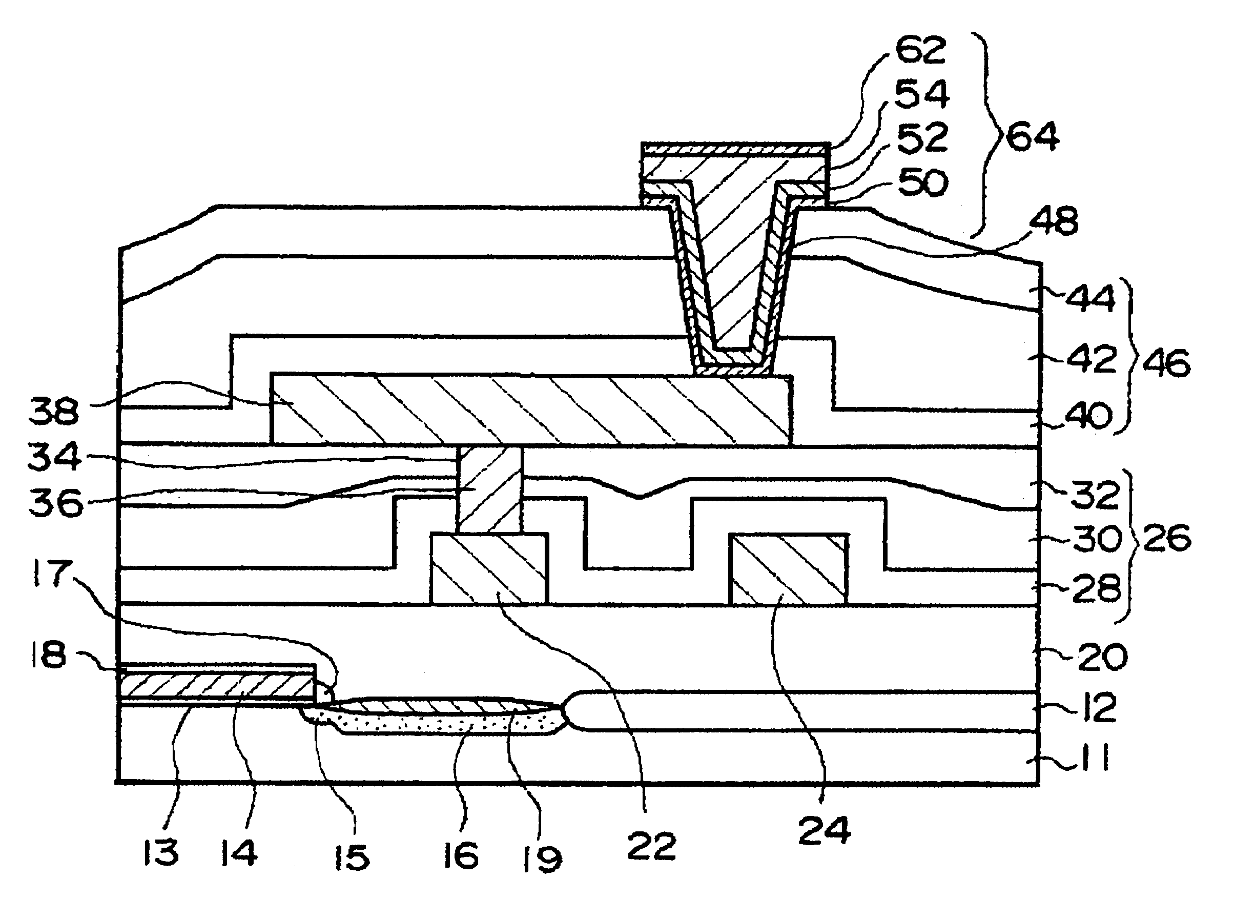
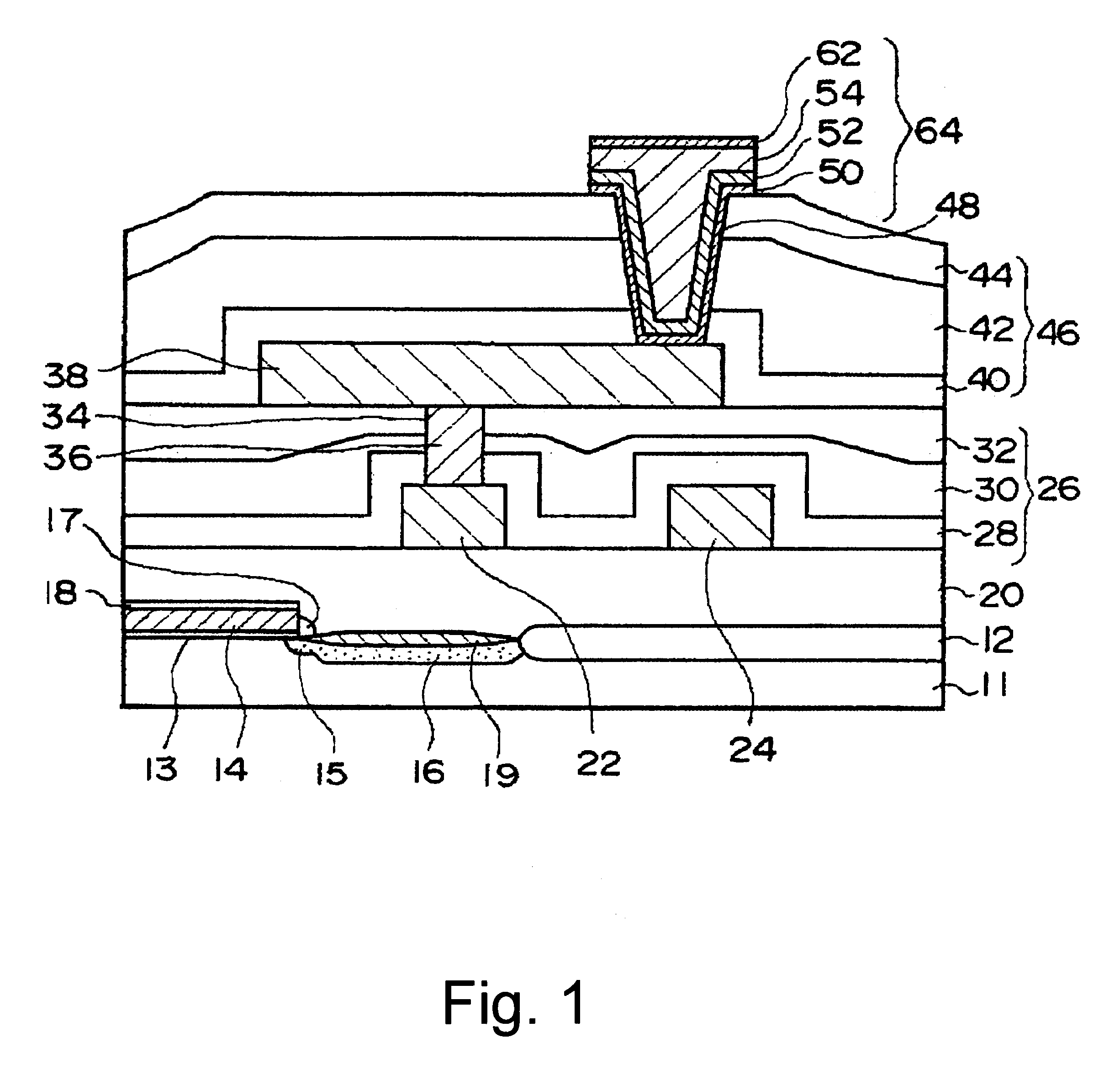
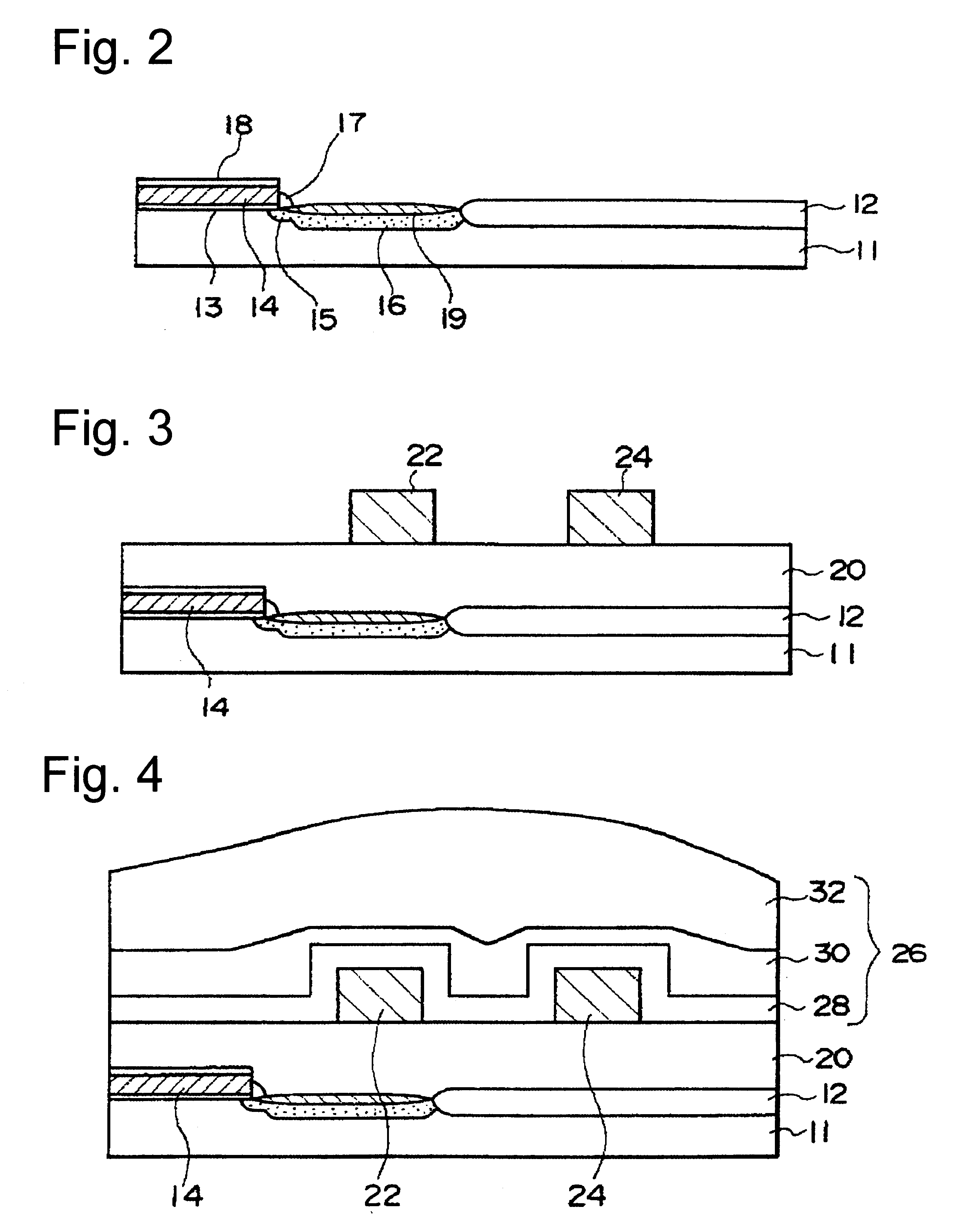
FIG. 1 is a cross-sectional view of a structure of a semiconductor device in accordance with a first embodiment of the present invention. First, the structure of the semiconductor device in accordance with the first embodiment of the present invention is briefly described. A silicon substrate 11 has a main surface, and on the main surface a MOS field effect transistor having a gate electrode 14 is formed. An interlayer dielectric film 20 is formed on the main surface of the silicon substrate 11 such that it covers the MOS field effect transistor. First metal wiring layers 22 and 24, which are spaced from each other, are formed on the interlayer dielectric film 20.

An interlayer dielectric film 26 is formed on the interlayer dielectric film 20 such that it covers the first metal wiring layers 22 and 24. The interlayer dielectric film 26 has an internal compression stress. A second metal wiring layer 38 is formed on the interlayer dielectric film 26. The first metal wiring layer 22 and...


PUM


Abstract

A semiconductor device has a structure that is capable of reducing warping of a semiconductor wafer when the semiconductor device is manufactured. The semiconductor device is manufactured by a method including the steps for forming an interlayer dielectric film having an internal compression stress and an interlayer dielectric film having an internal tensile stress. As a result, when semiconductor devices are manufactured, the tensile stress and the compression stress act on the semiconductor wafer. As a consequence, the overall stress that acts on the semiconductor wafer are reduced to a small level or to zero, and thus warping of the semiconductor wafer is reduced or eliminated when semiconductor devices are manufactured.

Description

1. Field of the InventionThe present invention relates to a semiconductor device having a multiple-wiring-layer structure and a method for manufacturing the same.2. Description of Related ArtIn a semiconductor device having a multiple-wiring-layer structure, insulation between wiring layers is provided by interlayer dielectric films. Techniques for forming interlayer dielectric films are described in, for example, Japanese Laid-open patent applications HEI 7-86284 and HEI 7-161703.These interlayer dielectric films disclosed in the above references have internal compression stress. This results in warping of a semiconductor wafer when semiconductor devices are manufactured. The warping of the semiconductor wafer creates various problems in manufacturing of semiconductor devices. For example, a semiconductor wafer is mounted on a vacuum chuck while thin films (interlayer dielectric films, metal wiring layers, etc.) are formed. If the semiconductor wafer is warped, heat is not uniforml...

Claims


Application Information

Patent Timeline
Patent Type & Authority Patents(United States)
IPC IPC(8): H01L21/02H01L21/768H01L21/285H01L21/70H01L21/316H01L23/522
CPCH01L21/2855H01L21/76801H01L21/76804H01L21/76828H01L21/76843H01L21/76864H01L21/76876H01L21/76882H01L21/31612H01L21/31625H01L21/02164H01L21/02274H01L21/02211H01L21/02203H01L21/022H01L21/02337
Inventor MOROZUMI, YOKIO
Owner SEIKO EPSON CORP
Why Eureka
Try Eureka