
Method for fabricating CMOS transistors having matching characteristics and apparatus formed thereby

a technology of cmos transistor and matching characteristics, which is applied in the direction of electrical equipment, basic electric elements, and semiconductor devices, etc., can solve the problems of excessive power dissipation, more difficult control of active and parasitic device threshold voltage, and improve the pull-up switching speed self-defea

Inactive Publication Date: 2002-08-20
APTINA IMAGING CORP
View PDF2 Cites 106 Cited by
  • Summary
  • Abstract
  • Description
  • Claims
  • Application Information

AI Technical Summary

Problems solved by technology

However, because non-idealities tend to shift the threshold voltage toward negative biases, early NMOS transistors were typically of the depletion mode type.
This was a particularly important consideration for NMOS technologies, which were gaining favor, in that high surface state charge density makes it more difficult to control active and parasitic device threshold voltages.
Not only does the asymmetrical switching slow circuit response, but a DC path exists from the power supply to ground during a significant portion of the slow switching transient resulting in excess power dissipation.
If the PMOS transistors, as is often done, are made two to three times larger than the NMOS devices, then extra stray capacitances are introduced which tend to make efforts to improve the pull-up switching speed self defeating and to result in extra power dissipation.
Moreover, such architecture does not effectively utilize chip area in circuit layouts.
CMOS technologies provide both n- and p-channel devices in one chip, at the expense of some increase in fabrication complexity and use of chip area as compared to simple NMOS transistors.
Consequently, average power consumption is usually much smaller for CMOS than for NMOS devices.

Method used


Image

  • Method for fabricating CMOS transistors having matching characteristics and apparatus formed thereby
  • Method for fabricating CMOS transistors having matching characteristics and apparatus formed thereby
  • Method for fabricating CMOS transistors having matching characteristics and apparatus formed thereby

Examples


Embodiment Construction

Illustrative embodiments and exemplary applications will now be described with reference to the accompanying drawings.

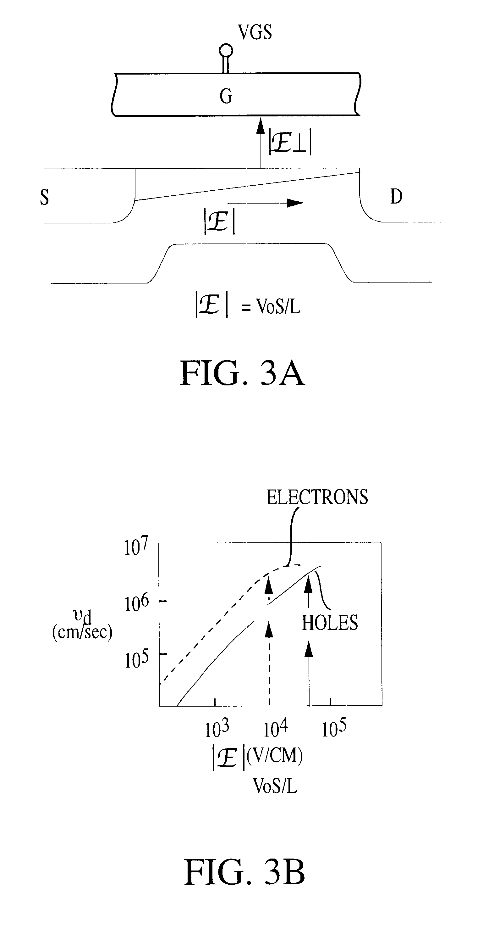
FIG. 5 illustrates the electron mobility of (111) silicon surfaces while FIG. 6 illustrates the hole mobility of (111) silicon surfaces, both under typical vertical electric fields due to the gate bias. The electron mobility is around 300 cm.sup.2 / V sec, which while lower than that on (100) surfaces, is still high enough to ensure velocity saturation on deep sub-micron devices, which might typically have drain to source electric fields of 1 V over 0.1 microns or 10.sup.5 V / cm. As shown in FIG. 5, inversion layer hole mobility can be 80% or higher on the (111) silicon surfaces, nearly 200 cm.sup.2 / V sec, than on the (100) surfaces. In the typical operating region, velocity saturation of holes will also occur for PMOS devices operated in the deep sub-micron region. Typical source-drain fields of 10.sup.5 V / cm and a mobility of 200 cm.sup.2 / Vsec will result in veloci...


PUM


Abstract

A method for forming NMOS and PMOS transistors that includes cutting a substrate along a (111) orientation and fabricating deep sub-micron NMOS and PMOS transistors thereon. The complementary NMOS and PMOS transistors form a CMOS transistor pair. The transistors are preferably used in structures such a memory circuits, e.g., DRAMs, which are, in turn, used in a processor-based system. Ideally, the deep sub-micron NMOS and PMOS transistors are operated in velocity saturation for optimal switching operation.

Description

1. Field of the InventionThe present invention relates to a method for forming CMOS transistors having matching characteristics and the apparatus formed by the method. More particularly, the present invention relates to a method for forming the CMOS transistors in the (111) surface plane and enabling a velocity saturation of both transistors.2. Description of the Related ArtHistorically, (111) surface orientation wafers were the first mass produced for use in integrated circuit technology. Such orientations are the easiest and least expensive to produce and were still used until recently in bipolar circuit tecnology. Around 1970, however, MOS ("metal oxide semiconductor") technology changed to the currently used (100) surface orientation of the wafers. This change was made when NMOS ("n channel MOSFET") technology rather than PMOS ("p channel MOSFET") technology became common and before the advent of CMOS technology. FIGS. 1A-1B illustrate the surface planes (100) and (111) and (110...

Claims


Application Information

Patent Timeline
Patent Type & Authority Patents(United States)
IPC IPC(8): H01L29/78H01L29/02H01L29/66H01L21/8238H01L21/70H01L29/04
CPCH01L21/823807H01L29/045H01L29/78
Inventor FORBES, LEONARDNOBLE, WENDELL P.
Owner APTINA IMAGING CORP
Features
  • Generate Ideas
  • Intellectual Property
  • Life Sciences
  • Materials
  • Tech Scout
  • Unparalleled Data Quality
  • Higher Quality Content
  • 60% Fewer Hallucinations
Learn More