Method and system for managing semiconductor manufacturing equipment

a semiconductor manufacturing and equipment management technology, applied in the direction of ignition automatic control, electric controllers, instruments, etc., can solve the problems of inability to capture time-series changes between data values, inability to detect equipment malfunctions accurately, and inability to use plasma emission intensity as a parameter to detect equipment malfunctions

Inactive Publication Date: 2002-08-20
LAPIS SEMICON CO LTD
View PDF9 Cites 61 Cited by
  • Summary
  • Abstract
  • Description
  • Claims
  • Application Information

AI Technical Summary

Benefits of technology

The object of the present invention is to provide a management method and a management system capable of making a correct decision about a malfunction of the semiconductor manufacturing equipment.
According to the present invention, the arithmetic circuit calculates a Mahalanobis distance from parameter values obtained by the detection mechanism on the basis of a Mahalanobis space stored in the memory unit, and the decision circuit decides whether or not the calculated Mahalanobis distance exceeds a predetermined value. Therefore, the method according to the present invention can be put into quick and effective use.
The emission spectrometer, being capable of measuring the intensity of a plurality of desired wavelengths, can handle the different degrees of intensity of the plurality of wavelengths of plasma emission as parameters. Therefore, it becomes possible to suitably manage the operating condition of the etching system by time series control according to the correlation between the different degrees of intensity of different wavelengths of plasma emission.

Problems solved by technology

However, in a conventional interlock system such as mentioned above, when the etching steps from beginning to end of etching work on a plasma etching system are controlled according to changes in the plasma emission intensity, the plasma emission intensity varies greatly from beginning to end of the etching process, so that the plasma emission intensity cannot be used as a parameter to detect a malfunction of the equipment.
In the interlock system, only one decision is made whether or not data values of a single parameter exceed a predetermined range, and it is impossible to capture time-series changes between data values.
Therefore, it is not easy to catch a malfunction accurately.
Further, in the interlock system, even if a plurality of parameters are combined, it is hard to give correlation between the parameters, and it is difficult to catch a malfunction accurately.

Method used


Image

  • Method and system for managing semiconductor manufacturing equipment
  • Method and system for managing semiconductor manufacturing equipment
  • Method and system for managing semiconductor manufacturing equipment

Examples


second embodiment

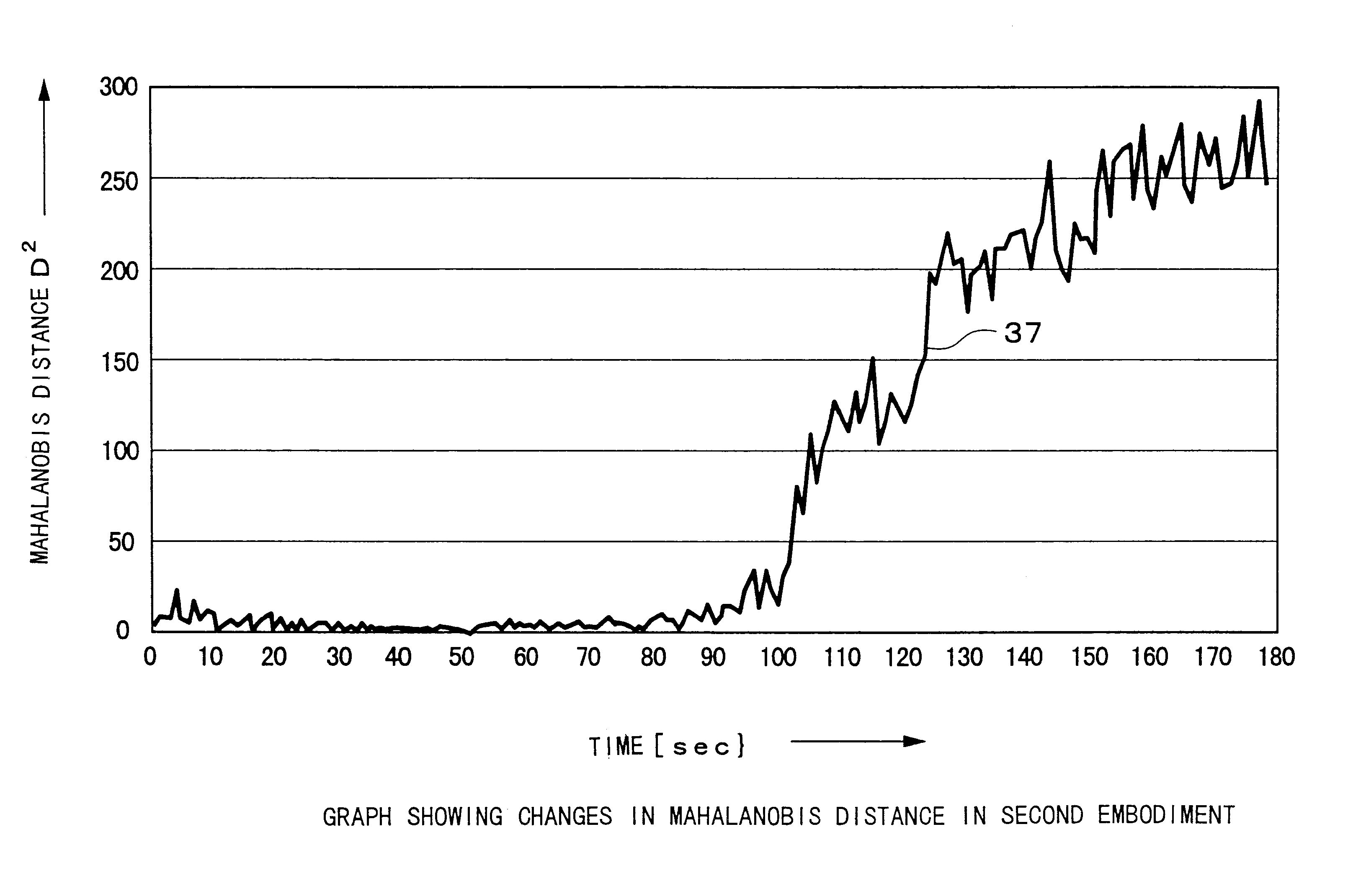
FIGS. 7 to 11 are graphs showing examples of changes in measured data (I.sub.0, I.sub.2, I.sub.3, I.sub.4, V.sub.1, V.sub.2, V.sub.3, V.sub.4 and the phase .THETA.) and changes in the Mahalanobis distance D.sub.2 in the second embodiment shown in FIG. 5.

This is a case where abnormality occurred in the operation of the plasma etching system 11 about 90 to 100 sec after the start of the etching process.

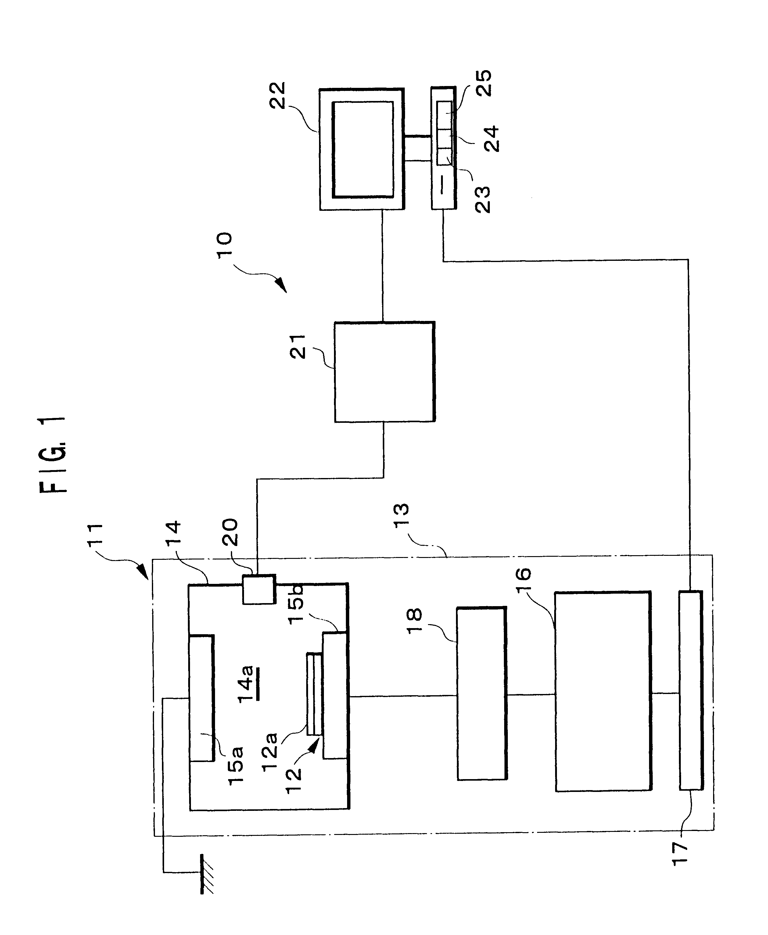
The horizontal axis of a graph in FIG. 7 represents time (sec) from the start to the end of etching, and the vertical axis represents voltage values [V]. The characteristic curves 26 and 27 respectively show changes in the voltage value V.sub.0 of the fundamental wave component and the voltage value V.sub.1 of the first harmonic component of high frequency output from the high frequency generator 16.

In the two characteristic curves 26 and 27, minute voltage changes are observed which are considered to be noise, but in the graph of FIG. 7, there are no notable indications of change other...

third embodiment

Therefore, the management system in the third embodiment is capable of detecting an infinitesimal change in plasma in the reaction chamber 14a of the plasma etching system 11, which cannot be detected only from a change in emission intensity. Therefore, it becomes possible to manage the operation of the plasma etching system 11 with high accuracy.

The foregoing description has been made using an optical parameter related to plasma emission or electrical parameters, such as voltage, current and phase of high frequency electric power in order to manage the operation of the plasma etching system.

The present invention of this patent application is not limited to them, it is possible to adopt various system parameters representing the operating condition of the plasma etching system, such as gas pressure, APC, or the like of the reaction chamber of the plasma etching system by using a detector, such as a mass spectrograph.

Besides the above-mentioned management of the plasma etching system...


PUM


Abstract

A management method capable of making an accurate decision about a malfunction of the semiconductor manufacturing equipment includes sampling a plurality of data of at least one parameter under normal operating conditions of the semiconductor manufacturing equipment; generating a Mahalanobis space A from a group of sampled data; calculating a Mahalanobis distance D.sup.2 from measured values of the parameter under ordinary operating conditions of the semiconductor manufacturing equipment; and deciding that a malfunction occurred in the semiconductor manufacturing equipment when the value of the Mahalanobis distance exceeds a predetermined value.

Description

BACKGROUND OF THE INVENTION1. Field of the InventionThe present invention relates to a method and a system for managing semiconductor manufacturing equipment.2. Related ArtIn management systems for manufacturing equipment, such as semiconductor manufacturing equipment, to decide whether or not the manufacturing equipment is operating normally, an interlock system is generally adopted which detects data on a parameter such as the temperature or pressure of the functional part of the manufacturing equipment, and stops the operation of the manufacturing equipment when the data indicates an abnormal value.According to this interlock system, it is possible to immediately stop the operation of the manufacturing equipment when an abnormal data value is detected, and thereby minimize the ejection of nonconforming products.However, in a conventional interlock system such as mentioned above, when the etching steps from beginning to end of etching work on a plasma etching system are controlled...

Claims


Application Information

Patent Timeline
Patent Type & Authority Patents(United States)
IPC IPC(8): G06F19/00H01L21/02
CPCG05B23/024H01J37/32935
Inventor HAYASHI, SHUNJI
Owner LAPIS SEMICON CO LTD
Why Eureka
Try Eureka