Column-row addressable electric microswitch arrays and sensor matrices employing them

an electric microswitch and column-row address technology, applied in the field of electric microswitch, can solve the problems of large size, often too slow switching speed of switches made with discrete mechanical relays, and material and process costs that limit the use of active matrix arrays in large-scale sensor applications

Inactive Publication Date: 2002-08-27
DUPONT DISPLAY +1
View PDF13 Cites 73 Cited by
  • Summary
  • Abstract
  • Description
  • Claims
  • Application Information

AI Technical Summary

Problems solved by technology

Switches made with discrete mechanical relays are too bulky, too large in size and often too slow in switching speed for this application.
However, the material and the process costs have limited the use of such active matrix arrays. in large size sensor applications.
However, the performance of these early devices (as determined by their I-V characteristics) was insufficient to enable use as electric switches.

Method used


Image

  • Column-row addressable electric microswitch arrays and sensor matrices employing them
  • Column-row addressable electric microswitch arrays and sensor matrices employing them
  • Column-row addressable electric microswitch arrays and sensor matrices employing them

Examples


example 1

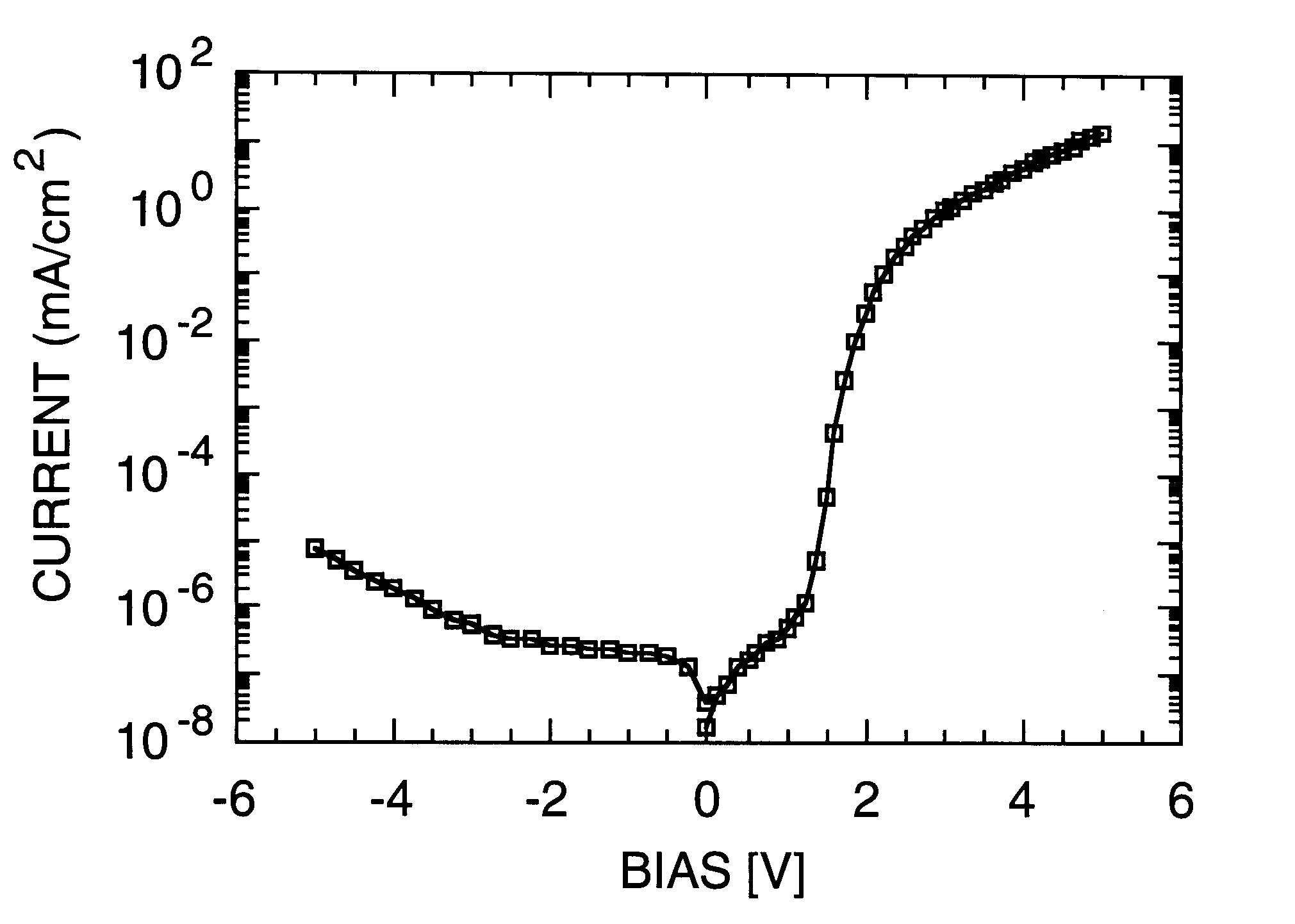
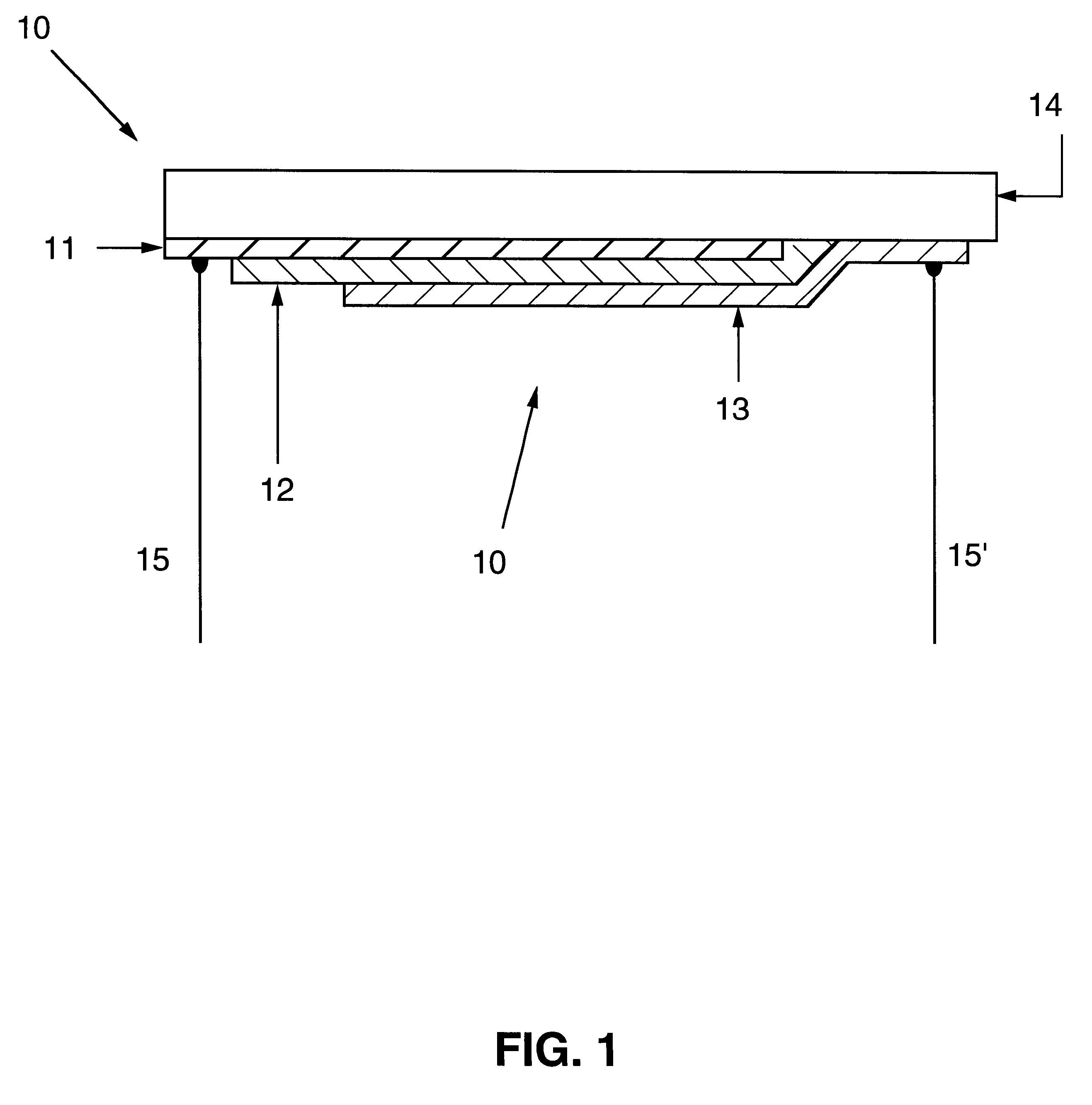
MSM devices were fabricated in the structure shown in FIG. 1. The anode electrode (11) used in this Example was an indium doped tin oxide (ITO) layer with work function close to 4.8 eV and surface resisitivity of .about.20 .OMEGA. / square. A 7 mil Mylar film was used as the substrate (14) for this device. A thin layer of MEH-PPV (.about.1500 .ANG.) was spin cast onto the ITO electrode at room temperature. Details on the synthesis and process of MEH-PPV can be found in literature [F. Wudl, P. M. Allemand, G. Srdanov, Z. Ni, and D. McBranch, in Materials for Nonlinear Optics: Chemical Perspectives, Ed. S. R. Marder, J. E. Sohn and G. D. Stucky (American Chemical Society, Washington, D.C., 1991) p. 683]. A thin layer of Ca (500-5000 .ANG.) was then thermally evaporated as the cathode electrode (the Ca was typically over-covered by a protective layer Al). The active area of each device was 0.1 cm.sup.2.

FIG. 5A shows the device current as a function of bias voltage. Forward bias is define...

example 2

The experiments of Example 1 were repeated with Au as the anode and Al as the cathode. The device size was reduced to .about.0.0004 cm.sup.2, comparable to that of a pixel in a microswitch matrix for image sensor applications. The I-V characteristics and the rectification ratio are shown in FIGS. 6A and 6B. The rectification ratio and the ON / Off ratio at 5V and 0V were .about.5.times.10.sup.5 and >10.sup.7, respectively.

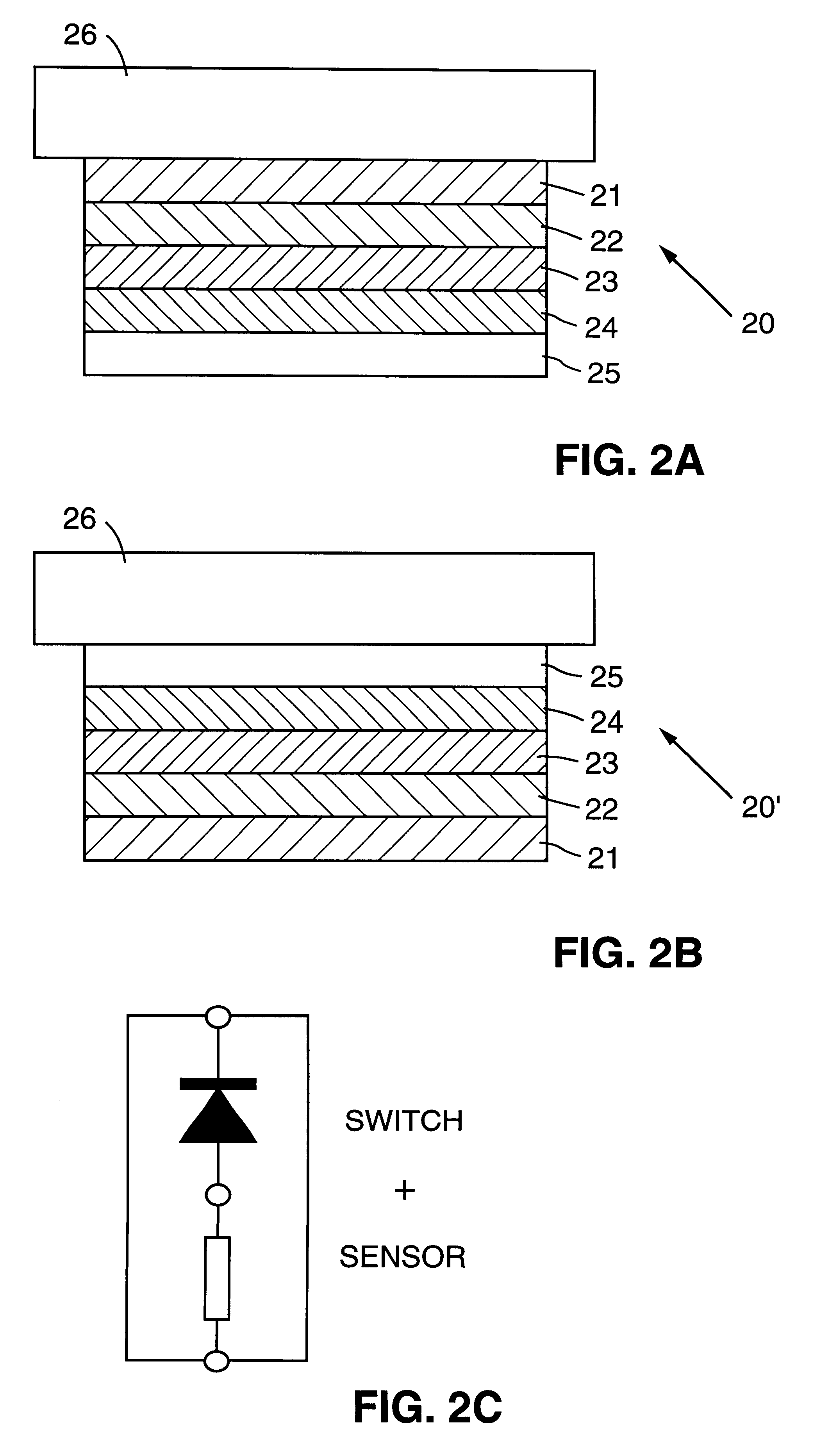
Similar devices were fabricated with different metal cathode, including Sm, Y, Pr, MgAg, MgAl, Li, Ba, Ag, Cu, In, Hf etc. Similar switching effect was observed in each case.

Similar devices were fabricated with a thin buffer inserting between the semiconducting layer and the cathode layer. Examples of the buffer layer include inorganic compounds such as LiF, BaO, BaF.sub.2, Li.sub.2 O. Organic molecules can also be used for the buffer. Examples include OCA mad its derivatives. Similar switching effect was observed in each case.

Organic molecules were also used for the...

example 3

The experiments of Example 1were repeated with ITO as the anode and Al as the cathode. An MeH-PPV:PCBM blend film (1:1 weight ratio) was used as the semiconducting layer 12, which was spin cast from solution in xylenes (concentration of approximately 0.5 wt %). PCBM is a fullerene molecule with molecular structure and chemical properties similar to C.sub.60 (a form of C molecule in buckyball shape). Details about its synthesis and characterization has been documented in literature [J. C. Hummelen, B. W. Knight, F. Lepec, and F. Wudl, J. Org. Chem. 60, 532 (1995)]. The I-V characteristics and the rectification ratio are plotted in FIGS. 7A and 7B. The rectification ratio was larger than 4.times.10.sup.5 for bias over 1.5 V and the ON / Off ratio operating at 2V and 0V was >3.times.10.sup.7.

Similar results were obtained from ITO / IAEH-PPV / C.sub.6 d / Al, ITO / TPB / Alq3 / Al devices in which the semiconducting layer was in a bi-layer structure reminiscent of the so-called heterojunction structu...


PUM

PropertyMeasurementUnit
current densitiesaaaaaaaaaa
temperatureaaaaaaaaaa

Abstract

The present invention relates generally to fabricating two-terminal electric microswitches comprising thin semiconductor films and using these microswitches to construct column-row (x-y) addressable microswitch matrices. These microswitches are two terminal devices through which electric current and electric potential (or their derivatives or integrals) can be switched on and off by the magnitude or the polarity of the external bias. The microswitches are made from semiconducting thin films in a electrode / semiconductor / electrode, thin film configuration. Column-row addressable electric microswitch matrices can be made in large areas, with high pixel density. Such matrices can be integrated with a sensor layer with electronic properties which vary in response to external physical conditions (such as photon radiation, temperature, pressure, magnetic field and so on), thereby forming a variety of detector matrices.

Description

1. Field of the InventionThe present invention relates generally to the fabrication of electric microswitches with thin semiconductor films and column-row (x-y) addressable electric switch matrices constructed with such microswitches. These microswitches are two terminal devices through which electric current, electric potential or their derivatives or integrals can be switched on and off by the magnitude or the polarity of an external bias. They are made of semi conducting thin films in metal / semiconductor / metal, thin film configuration. Column-row addressable electric micro-switch matrices can be made to cover large areas, with high pixel density. Such matrices can be integrated with one (or several) additional layer(s) with electronic properties which vary in response to external physical conditions (such as photon radiation, temperature, pressure, x-rays, magnetic field and so on), thereby forming a variety of detector matrices.2. Brief Description of the Prior ArtTraditional el...

Claims


Application Information

Patent Timeline
Patent Type & Authority Patents(United States)
IPC IPC(8): H01L27/28H01L27/144H01L27/30H01L27/146H01L51/05H01L51/30G01J1/02H01L21/00H01L27/24H01L29/47H01L29/872H01L31/09H01L35/24H01L45/00H01L47/00H01L49/02H01L51/00H01L51/42
CPCB82Y10/00H01L27/1446H01L27/14609H01L27/14643H01L27/14667H01L27/14676H01L27/14687H01L27/28H01L27/285H01L27/30H01L27/307H01L27/308H01L51/0591H01L51/4206H01L51/0034H01L51/0035H01L51/0036H01L51/0037H01L51/0038H01L51/0041H01L51/0046H01L51/0047H01L51/0081H01L51/0583H01L51/424H01L51/4253Y02E10/549H10K19/202H10K19/00H10K39/00H10K39/36H10K39/32H10K85/10H10K85/113H10K85/143H10K85/111H10K85/1135H10K85/114H10K85/211H10K85/215H10K85/324H10K10/26H10K10/50H10K30/451H10K30/30H10K30/20H10K30/00
Inventor YU, GANGCAO, YONG
Owner DUPONT DISPLAY
Why Eureka
Try Eureka