Dicing tape and a method of dicing a semiconductor wafer

a technology of dicing tape and semiconductor wafer, which is applied in the direction of film/foil adhesives, manufacturing tools, transportation and packaging, etc., can solve the problems of excessive cumbersome adjustment of expanding apparatus, insufficient expansion of chip spacing, and torque applied by expanding apparatus, etc., and achieves the effect of rare breakage at the dicing lin

Inactive Publication Date: 2002-09-03
LINTEC CORP
View PDF5 Cites 48 Cited by
  • Summary
  • Abstract
  • Description
  • Claims
  • Application Information

AI Technical Summary

Benefits of technology

Accordingly, the object of the present invention is to remedy the defects in prior art, and provide a dicing tape which can uniformly and sufficiently enlarge dicing lines without affect by a modulus of elasticity of a pressure-sensitive adhesive, and is rarely broken at the dicing lines.

Problems solved by technology

It is extremely cumbersome to adjust the expanding apparatus by changing the stretching amount or the torque, each time a type of dicing tape to be treated is changed, or a size of a semiconductor wafer attached to the dicing tape is changed.
Under the above circumstances, when a substrate material of a dicing tape stretched on the expanding apparatus has a high ductility, a stretching stress is not conveyed to an area where a semiconductor wafer is attached, and thus the spacing of the chips is not sufficiently enlarged.
To the contrary, when a substrate material of a dicing tape being stretched has a low ductility, a stretching torque applied by the expanding apparatus becomes insufficient, the spacing of the chips is nonuniformly enlarged, or the dicing tapes may be broken.
The peripheral area is also stretched together with the central portion where dicing lines are formed, and therefore, a stretching torque applied by the expanding apparatus becomes insufficient, or in some cases the dicing tapes may be broken.
However, an expanding apparatus is required to have a high torque for enlarging the spacing of the chips.
When the pressure-sensitive adhesive has a low modulus of elasticity, a stress applied to a dicing tape in the expanding step is relaxed by a deformation of the pressure-sensitive adhesive, and thus the stress is not sufficiently conveyed to the dicing lines, and therefore, a sufficient spacing of the chips is not obtained.

Method used


Image

  • Dicing tape and a method of dicing a semiconductor wafer
  • Dicing tape and a method of dicing a semiconductor wafer

Examples


example 1

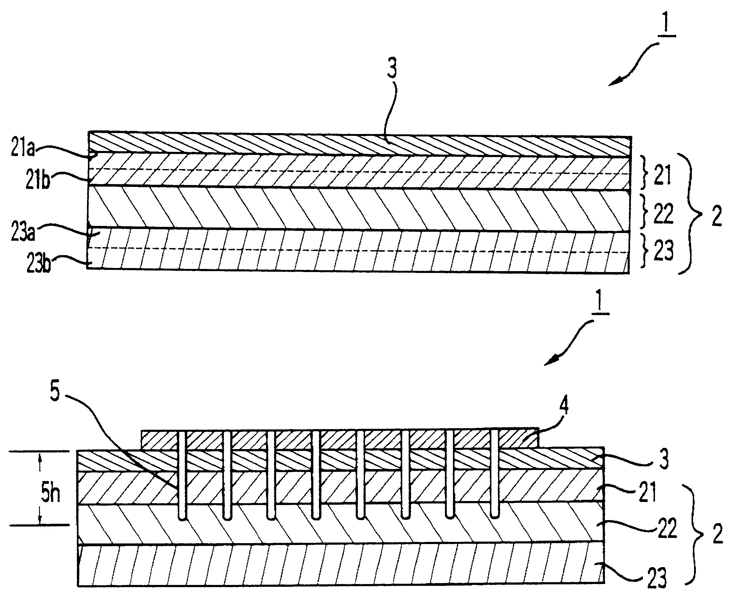
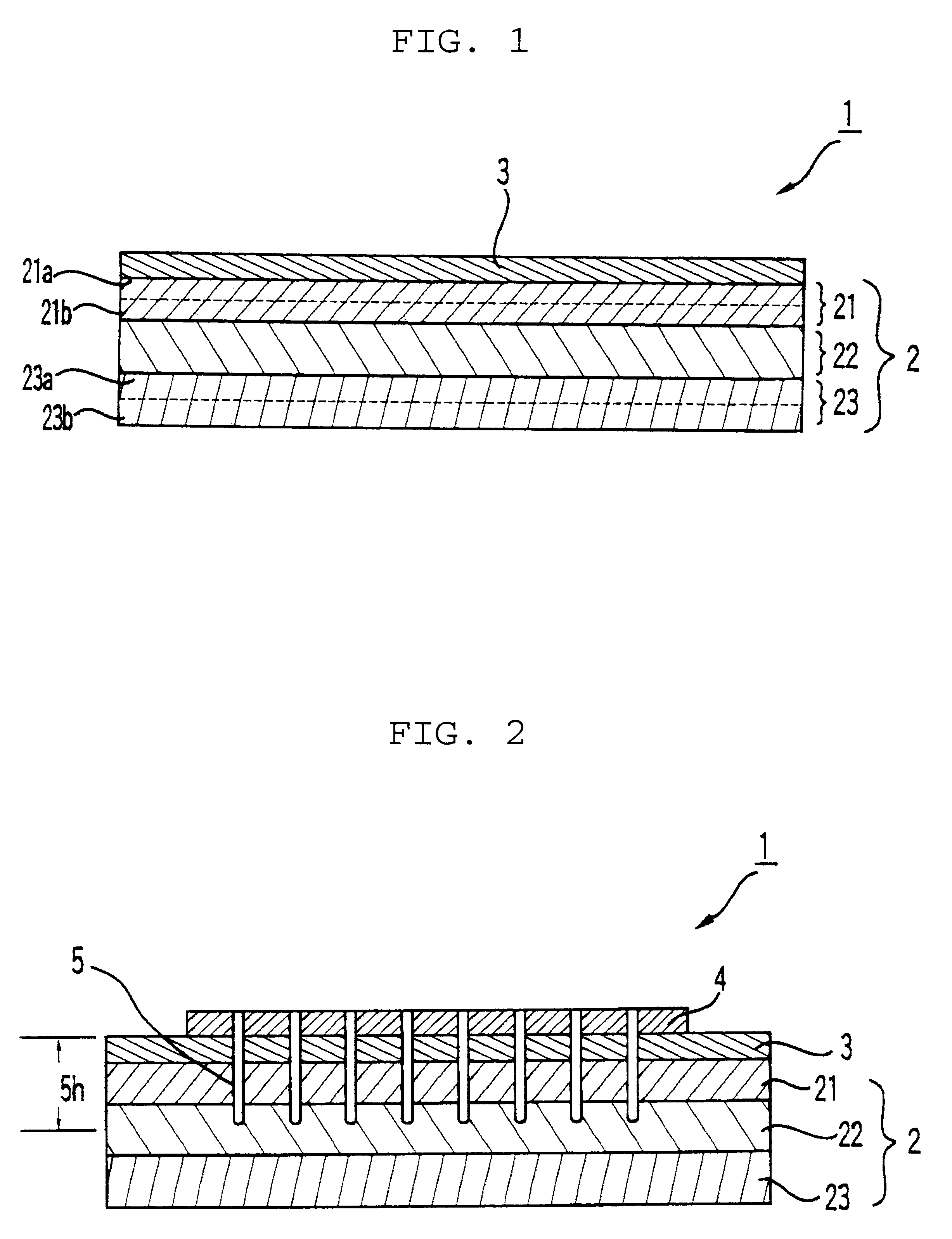
In the present Example, a dicing tape 1 of the present invention was manufactured. In the dicing tape 1, a pressure-sensitive adhesive layer 3 was laminated on an upper layer 21 of a substrate sheet 2 composed of the upper layer 21, an intermediate layer 22 and a lower layer 23.

A pressure-sensitive adhesive used for forming the pressure-sensitive adhesive layer 3 was an acrylate-based and UV-curable pressure-sensitive adhesive prepared by blending 125 parts by weight of polyfunctional urethane acrylate, 1 part by weight of multifunctional isocyanate compound and 5 parts by weight of photopolymerization initiator to 100 parts by weight of a copolymer compound having a weight-average molecular weight of 500,000 and prepared from butyl acrylate / methyl methacrylate / 2-hydroxyethyl acrylate (50 parts by weight / 45 parts by weight / 5 parts by weight).

As the upper layer 21, an ethylene methacrylic acid copolymer film (methacrylic acid content=9%) was used. Further, an ethylene-vinyl acetate c...

example 2

In the present Example, a dicing tape 1 of the present invention wherein a pressure-sensitive adhesive layer 3 was laminated on an upper layer 21 of a substrate sheet 2 was manufactured. The substrate sheet 2 was composed of an upper layer having two upper sublayers, an intermediate layer 22 and a lower layer 23 which layers were laminated in this sequence. The UV-curable pressure-sensitive adhesive used in Example 1 was used to form the pressure-sensitive adhesive layer 3. Table 1 shows the films, modulus of elasticity and layer thicknesses of the layers.

The dicing tape 1 of the present invention was manufactured by repeating the procedure described in Example 1, except that the film compositions were co-extruded from a four-layer co-extruder to form a four-layer substrate sheet 2. Table 3 shows the anti-extensibilities of the layers in the resulting dicing tape 1. The resulting dicing tape 1 was used in the dicing method as shown in Evaluation Example 1 mentioned later to determin...

example 3

In the present Example, a dicing tape 1 of the present invention, wherein a pressure-sensitive adhesive layer 3 was laminated on an upper layer 21 of a substrate sheet 2, was manufactured. The substrate sheet 2 was composed of the upper layer 21, an intermediate layer 22 and a lower layer 23 having two lower sublayers. These layers were laminated in this sequence. The UV-curable pressure-sensitive adhesive used in Example 1 was used to form the pressure-sensitive adhesive layer 3. Table 1 shows the films, modulus of elasticity and layer thicknesses of the layers.

The dicing tape 1 of the present invention was manufactured by repeating the procedure described in Example 1, except that the film compositions were co-extruded from a four-layer co-extruder to form a four-layer substrate sheet 2. Table 3 shows the anti-extensibilities of the layers in the resulting dicing tape 1. The resulting dicing tape 1 was used in the dicing method as shown in Evaluation Example 1 mentioned later, to ...


PUM

PropertyMeasurementUnit
cutting depthaaaaaaaaaa
thicknessaaaaaaaaaa
thicknessaaaaaaaaaa

Abstract

A dicing tape comprising a substrate sheet and a pressure-sensitive adhesive layer formed on one surface of the substrate sheet, wherein the substrate sheet comprises an upper layer in direct contact with the pressure-sensitive adhesive layer, an intermediate layer adjacent to the upper layer, and a lower layer adjacent to the intermediate layer, and an anti-extensibility (A) of the upper layer, an anti-extensibility (B) of the intermediate layer, and an anti-extensibility (C) of the lower layer satisfy the equation (I): the anti-extensibility being a product of a modulus of elasticity and a layer thickness, is disclosed. The present dicing tape can uniformly and sufficiently enlarge dicing lines without affect by a modulus of elasticity of a pressure-sensitive adhesive, and is rarely broken at the dicing lines.

Description

BACKGROUND OF THE INVENTION1. Field of the InventionThe present invention relates to a dicing tape and a method of dicing a semiconductor wafer wherein the dicing tape is used.2. Description of the Related ArtIn successive steps of manufacturing semiconductor chips, in a dicing step a dicing tape is used to fix a semiconductor wafer thereon, and the semiconductor wafer is then cut into individual chips. The dicing step is followed by expanding, picking-up and mounting steps.In the expanding step, the dicing tape is expanded to thereby expand or extend the widths of dicing lines or cutting lines formed in the dicing step and thus enlarge the spacing of the chips. The purpose of enlarging the spacing of the chips in the expanding step is to enhance a recognizability of the chips and to prevent the chips from coming into contact with adjacent chips and being damaged, when picked up in the picking-up step.Nowadays, in the expanding step an expanding apparatus is used to stretch the dici...

Claims


Application Information

Patent Timeline
Patent Type & Authority Patents(United States)
IPC IPC(8): B28D5/00C09J7/02H01L21/68H01L21/67H01L21/301C09J7/29
CPCB28D5/0082H01L21/6836C09J7/0296Y10T156/1052C09J2201/122C09J2201/162C09J2201/606C09J2203/326C09J2423/006C09J2433/00H01L2221/68327Y10T428/2848Y10T156/1064Y10T156/1082Y10T156/1026Y10T428/28C09J7/29C09J2301/162C09J2301/122C09J2301/302H01L21/30
Inventor SENOO, HIDEOKONDO, TAKESHI
Owner LINTEC CORP
Why Eureka
Try Eureka