Loadless static random access memory device and method of manufacturing same

a random access memory and static random access technology, applied in the direction of semiconductor devices, electrical devices, transistors, etc., to achieve the effect of preventing soft errors

Inactive Publication Date: 2002-09-24
RENESAS ELECTRONICS CORP
View PDF10 Cites 15 Cited by
  • Summary
  • Abstract
  • Description
  • Claims
  • Application Information

AI Technical Summary

Benefits of technology

As a result, when the power-source potential is applied to the gate electrodes of the address-selecting MOS transistors during standby, loss of electric charge is compensated for by passing a sub-threshold current through these transistors, whereby an output node of the driving transistors can be maintained at the power-source potential. Thus, resultant compensation for loss of charge in the memory cell makes it possible to retain data.
It is another object of the present invention to improve the operating stability of the semiconductor memory device and effectively suppressing soft error, and in which the threshold-voltage value can be control led freely in the case of a 4-transistor SRAM not having high-resistance load elements.
In accordance with the present invention, adjustment of the impurity concentration of the p well in a memory cell and formation of a deep n well can be carried out with a single resist pattern. This makes it possible to eliminate a PR step for forming a deep n well for the purpose of preventing soft error caused by alpha rays entrant from the outside.
Further, in accordance with the present invention, the reference potential of the p-we II region of the memory cell can be controlled freely in a loadless 4-transistor SRAM. As a result, data that has been stored in the memory cell can be retained in reliable fashion.

Problems solved by technology

These challenges give rise to the problems described below.

Method used


Image

  • Loadless static random access memory device and method of manufacturing same
  • Loadless static random access memory device and method of manufacturing same
  • Loadless static random access memory device and method of manufacturing same

Examples


first embodiment

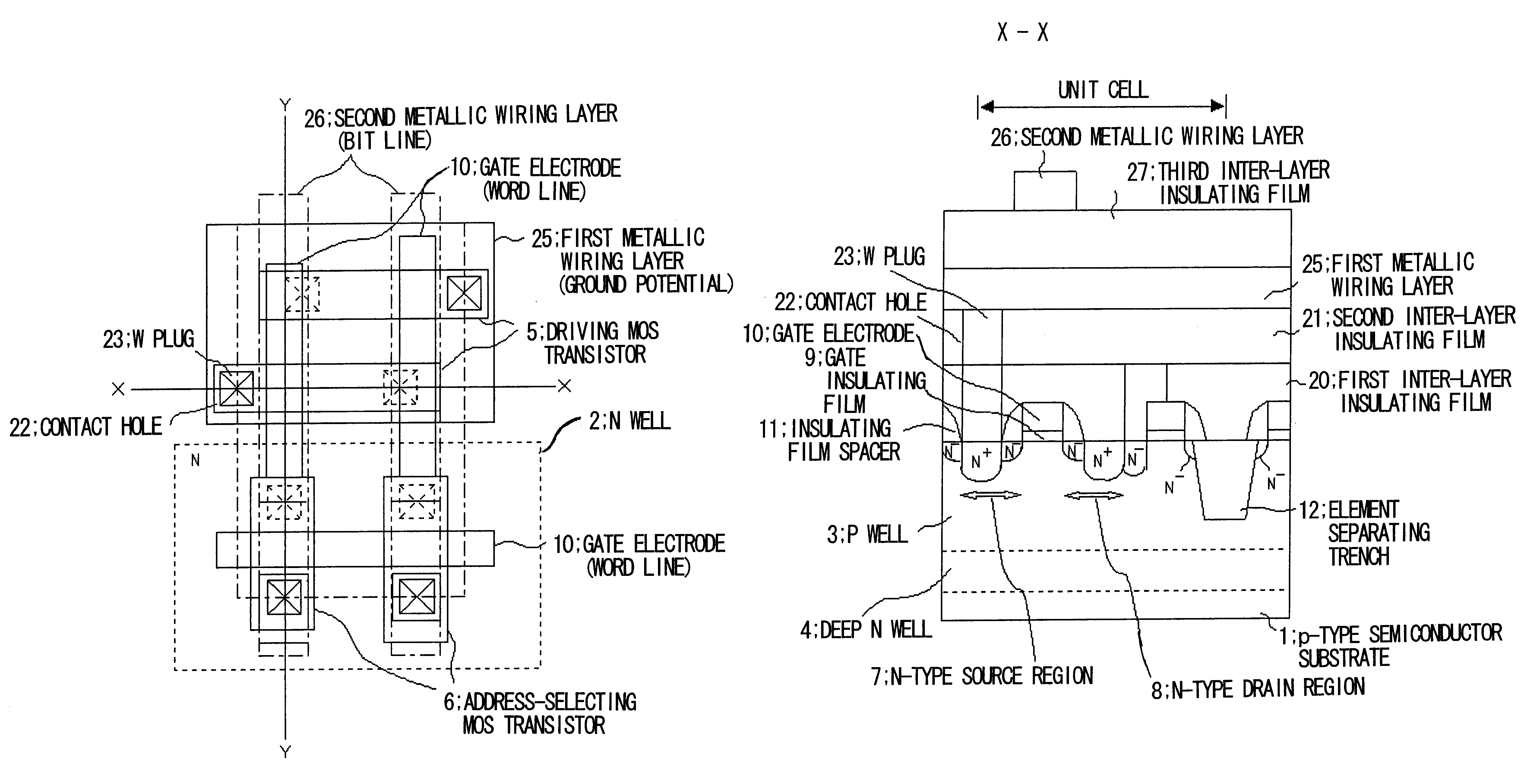
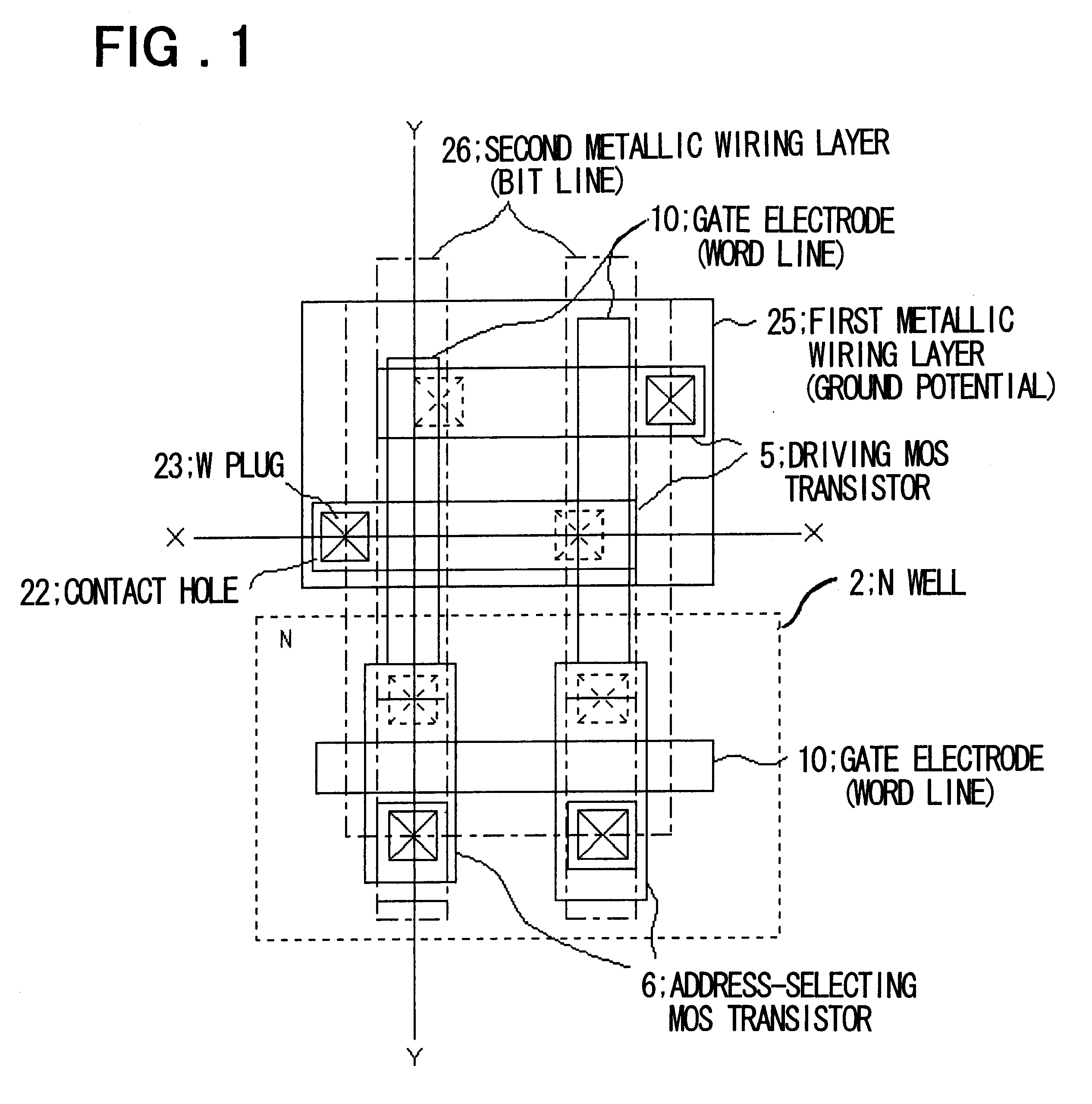
A semiconductor memory device according to first embodiment of the present invention will be described with reference to FIGS. 1 to 8. FIG. 1 is a plan view illustrating the construction of a loadless 4-transistor SRAM according to the first embodiment, FIG. 2 a sectional view taken along line X--X of FIG. 1 and FIG. 3 a sectional view taken along line Y--Y of FIG. 1. FIGS. 4 to 6 are process sectional views in which a method of manufacturing the semiconductor memory device is illustrated in the order of the steps. Furthermore, FIGS. 4(a) to 6(g) illustrate a series of manufacturing steps, which are shown as individual diagrams for convenience sake. FIG. 7 is a diagram useful in describing the steps of FIGS. 4(c) to 5(d), which deal particularly with an SRAM cell area. FIG. 8 is a diagram useful in describing a loadless SRAM formed by the method of this embodiment.

The construction of the semiconductor memory device according to this embodiment will be described first. As depicted in...

second embodiment

A semiconductor memory device according to a second embodiment of the present invention will be described with reference to FIGS. 9 to 11. FIG. 9 is a process sectional view schematically illustrating part of a method of manufacturing the semiconductor memory device according to this embodiment. FIG. 10 is a sectional view schematically illustrating the structure of the semiconductor memory device according to this embodiment, and FIG. 11 is a sectional view in a case where the method of forming the deep n well of this embodiment is applied to a DRAM. It should be noted that this embodiment differs from the first embodiment in that the deep n well of this embodiment is formed so as to cover only that part of the memory cell underlying the p well. Other steps of the manufacturing process and other components are the same as those of the first embodiment.

With regard to the process for forming the deep n well characterizing this embodiment, steps up to the formation of the p well and n...

third embodiment

A semiconductor memory device according to a third embodiment of the present invention will be described with reference to FIG. 12, which is a process sectional view schematically illustrating part of a method of manufacturing a semiconductor memory device according to the third embodiment. This embodiment differs from the second embodiment in that the shape of the resist pattern in this embodiment is the usual rectangular shape, the characterizing feature being that the injection (implantation) angle of ions in the step for forming the deep n well is set to an angle less than 90.degree. . Other steps of the manufacturing process and other components are the same as those of the second embodiment.

With regard to the process for forming the deep n well characterizing this embodiment, which will be described with reference to FIG. 12, steps up to the well formation of FIG. 4(b) are carried out through a method similar to that of the first embodiment described above, after which the res...


PUM


Abstract

A plurality of p wells and a plurality of n wells are formed in a p-type semiconductor substrate having a memory portion and a peripheral circuit portion. Next, a resist pattern is formed on the semiconductor substrate. The resist pattern has apertures which, as viewed from the direction normal to the plane of the semiconductor substrate, approximately coincide with the p wells, wherein the area of aperture openings on the top side of the resist pattern is different from the area of aperture openings on the bottom side of the resist pattern. By using the resist pattern as a mask, p-type ions are injected in a shape approximately the same as that of the aperture opening on the top side or bottom side, whichever has the smaller area. Thereafter, by using the same resist pattern as a mask, n-type ions having enough energy to pass through resist of a predetermined thickness are injected into the p-type semiconductor substrate through areas, located adjacent the apertures in the resist pattern, in which the effective thickness of the resist is small, thereby forming deep n wells so as to cover the p well regions.

Description

This invention relates to a semiconductor memory device and to a method of manufacturing the same. More particularly, the invention relates to a semiconductor memory device ideal for use in a semiconductor memory comprising an SRAM (Static Random-Access Memory), and to a method of manufacturing the device.Memories well-known in the art and typified by LSI circuits (Large-Scale Integrated Circuits) are classified into SRAMs and DRAMs (Dynamic Random-Access Memories). Almost all of these memories are constituted by MOS (Metal-Oxide Semiconductor) transistors which excel in terms of degree of integration. Further, since SRAMs are advantageous in that they have a higher operating speed than DRAMs, they find wide application for use particularly in memories such as cache memories requiring a high operating speed.An SRAM basically is constituted by a flip-flop circuit. The flip-flop circuit employs a pair of MOS transistors for drive, in which the input and output electrodes of the transi...

Claims


Application Information

Patent Timeline
Patent Type & Authority Patents(United States)
IPC IPC(8): H01L21/70H01L27/11H01L21/8244H01L27/105H01L21/8238H01L21/8242H01L27/092H01L27/108
CPCH01L27/105H01L27/11H01L27/1112H01L27/1116Y10S257/903H10B10/15H10B10/00H10B10/18
Inventor NODA, KENJI
Owner RENESAS ELECTRONICS CORP
Why Eureka
Try Eureka