Processing apparatus and a processing method

a processing apparatus and processing method technology, applied in the direction of electrical apparatus, electrostatic charges, emergency protective arrangement details, etc., can solve the problems of the top and bottom faces of the substrate being charged with opposite polarities, and the difficulty of separation from the bas

Inactive Publication Date: 2002-09-24
TOKYO ELECTRON LTD
View PDF27 Cites 17 Cited by
  • Summary
  • Abstract
  • Description
  • Claims
  • Application Information

AI Technical Summary

Problems solved by technology

In particular, an LCD substrate constituted by a thin glass plate is easily warped, which makes its separation from the base difficult In addition, when the substrate is lifted above the base, the polarization effect may cause charges of opposite polarities on the top and bottom face of the substrate.

Method used


Image

  • Processing apparatus and a processing method
  • Processing apparatus and a processing method
  • Processing apparatus and a processing method

Examples


first embodiment

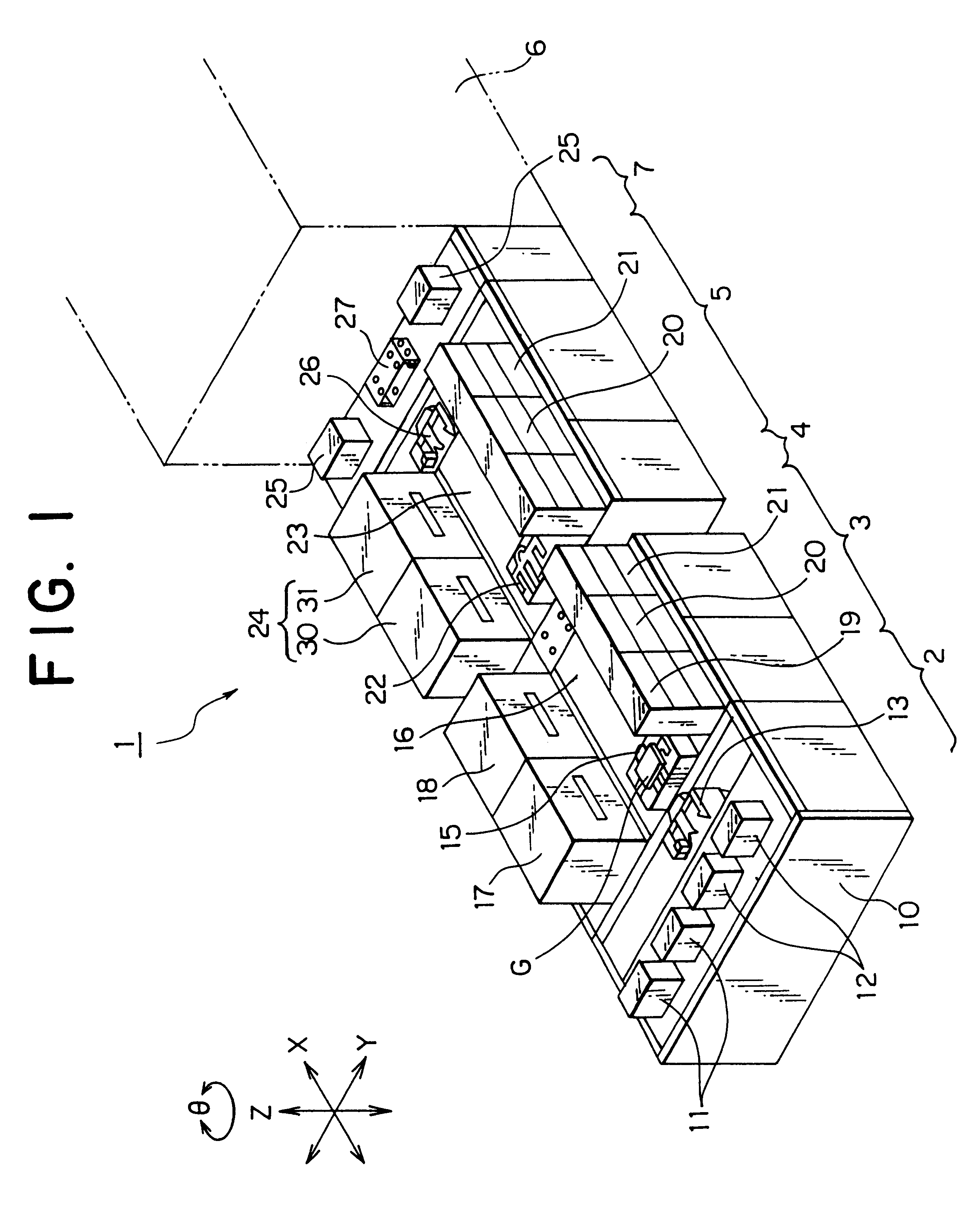
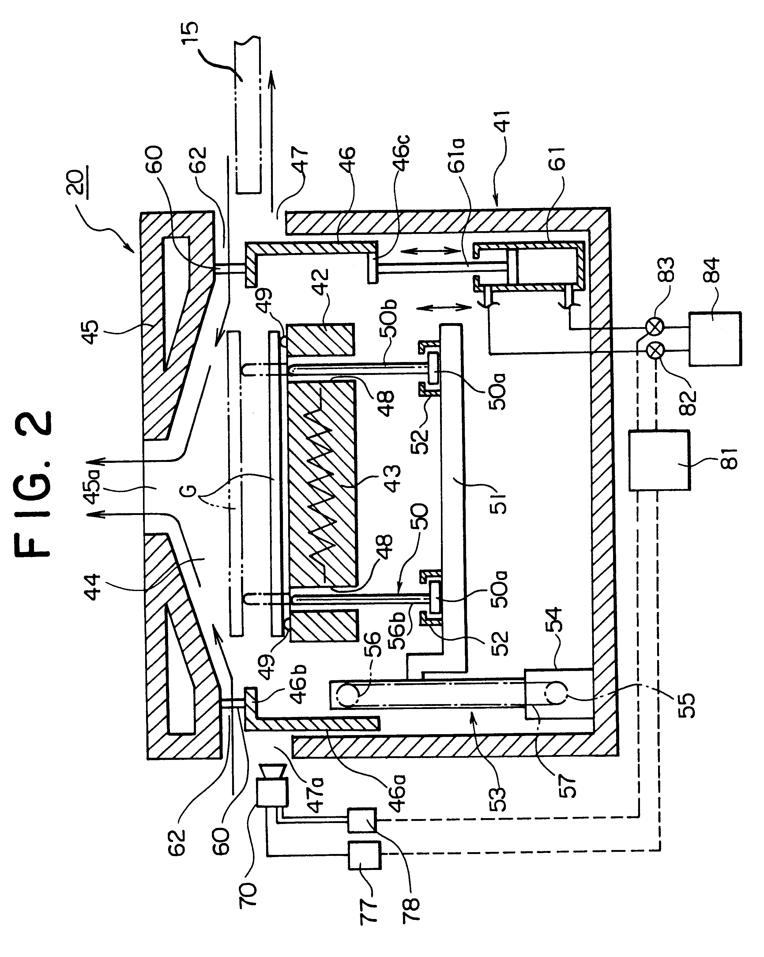
Referring to the attached figures, preferred embodiments of the present invention will be described below. FIG. 1 is a perspective view of a coater-developer system 1 to process the substrate using photo-lithography technology. The coater-developer system 1 is provided with a heater 20 as a processing apparatus according to a The coater-developer system 1 comprises a loader section 2 to carry in and out the LCD substrate G having a square shape for example, a first processing section 3 to process the LCD substrate G, a second processing section 5 installed in communication with the first processing section 3 via an interface section 4 and an interface section 7 to pass the LCD substrate G between the second processor 5 and, for example, an exposing apparatus 6.

The loader section 2 is provided with a cassette station 10. The cassette station 10 may freely have a plurality of cassettes 11 to store unprocessed LCD substrates G and a plurality of cassettes 12 to store processed LCD sub...

second embodiment

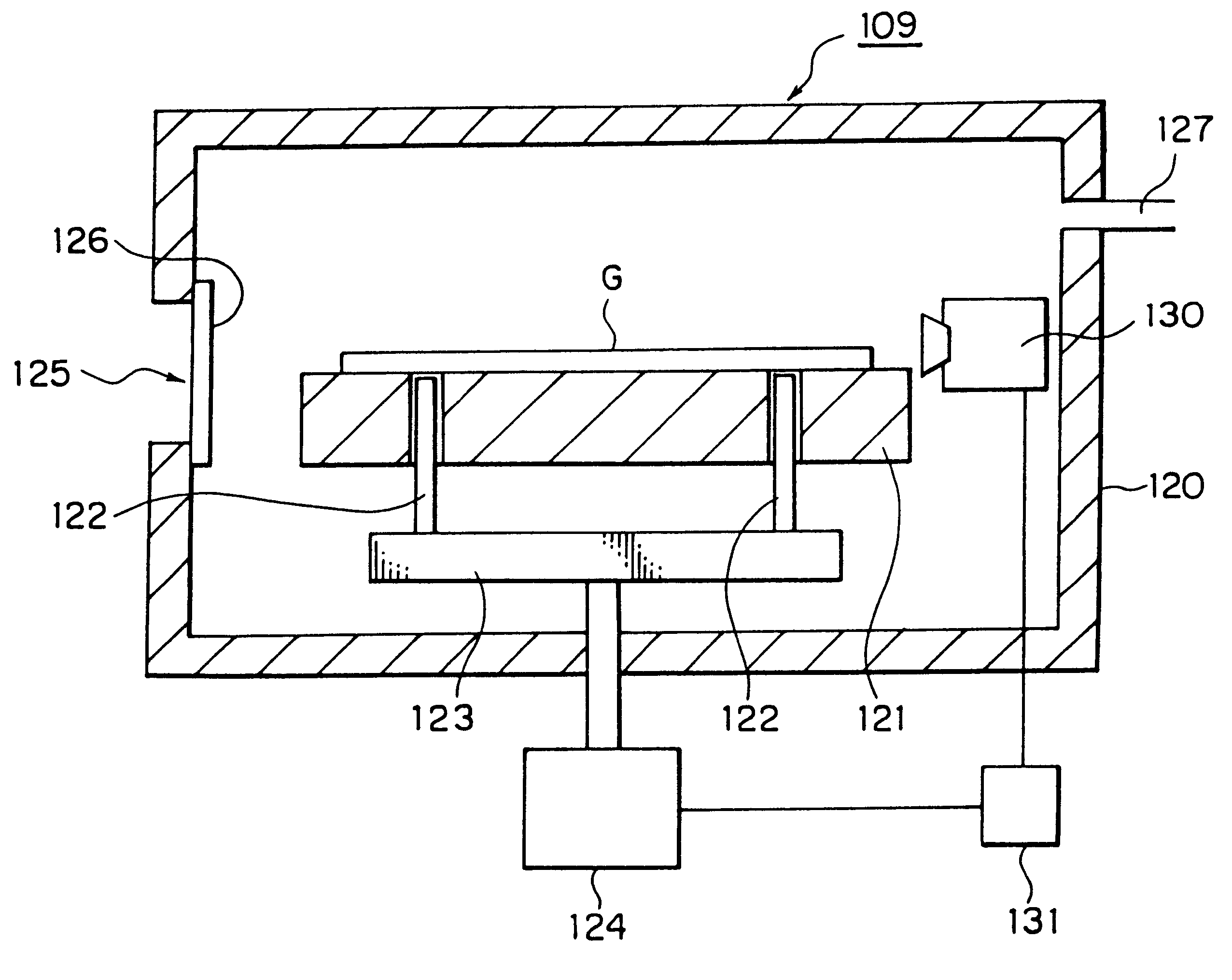
the present invention is described now. A resist processing system 101 shown in FIG. 9 is provided with a cassette station 103 on an end. The cassette station 103 has several cassettes 102 accommodating LCD substrates G (hereinafter referred to as the "substrate G") placed on it. Disposed on the front side of the cassettes 102 on the cassette station 103 is an auxiliary arm 105 which transfers and positions the substrate G and at the same time holds and passes the substrate G to and from main arms 104. Two main arms 104 are laid out in series so that they can move longitudinally at the center of the processing system 101. Developers 106 and other various processing apparatuses are disposed on both sides of the transfer route.

In the processing system 101 as shown in the figure, a brush scrubber 107 to clean the substrate G with a brush and a high pressure jet cleaner 108 to clean it with high pressure jet water are disposed side by side beside the cassette station 103. In addition, t...


PUM


Abstract

The processing apparatus prevents difficulty in separation of the substrate from the base because of charges on the substrate when the substrate is lifted from the base for substrate placing during processing. The processing apparatus comprises pins to lift up the substrate on the base and a neutralization apparatus to discharge ionized gas to the gap between the bottom of the substrate lifted from the base by the pins and the top of the base. When ionized gas is discharged to the substrate and the base, the charges are neutralized. In addition, the processing apparatus comprises three or more of proximity pins, which form gap between the bottom of the substrate on the base and the top of the base to prevent a frictional electricity being formed therein.

Description

1. Field of the InventionThe present invention relates to a processing apparatus and a processing method for processing to dry substrates such as, for example, LCD substrates or semiconductor wafers.2. Description of the Related ArtIn fabrication of liquid crystal displays (LCD) or semiconductors, the technology called "lithography" is applied to form resist patterns on the surface of the LCD substrate or semiconductor wafer serving as the bases. Lithography processing contains various processes such as substrate cleaning, substrate drying, resist application to: the substrate surface and exposure and development of such resist. In these processes, heaters are used for the above drying process, for example. As an example of such heaters, a apparatus to place a substrate on a base for substrate heating is known. Such a heater is provided with several pins projecting upward from the base to support the bottom of the substrate when the substrate is received and passed so that it receiv...

Claims


Application Information

Patent Timeline
Patent Type & Authority Patents(United States)
IPC IPC(8): H01L21/00
CPCH01L21/67017
Inventor HIROSE, OSAMUSADA, TETSUYA
Owner TOKYO ELECTRON LTD
Why Eureka
Try Eureka