

Electronic device having an active matrix display panel
a technology of active matrix and electronic equipment, applied in non-linear optics, instruments, optics, etc., can solve the problem of high manufacturing cos
- Summary
- Abstract
- Description
- Claims
- Application Information
AI Technical Summary
Problems solved by technology
Method used
Image

Examples
embodiment 1
[Embodiment 1]
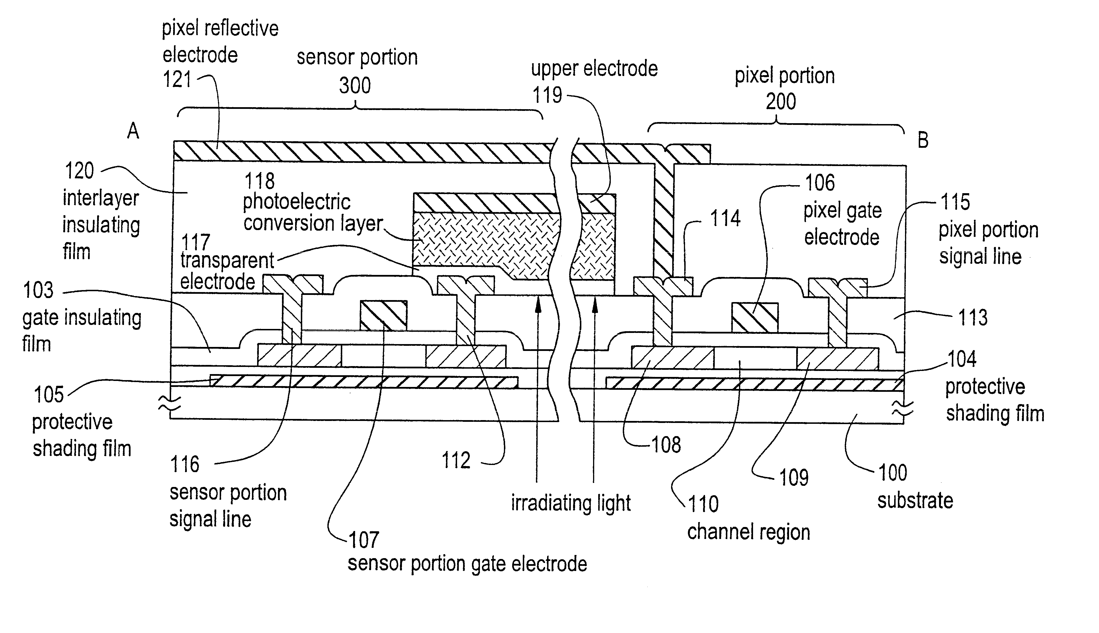
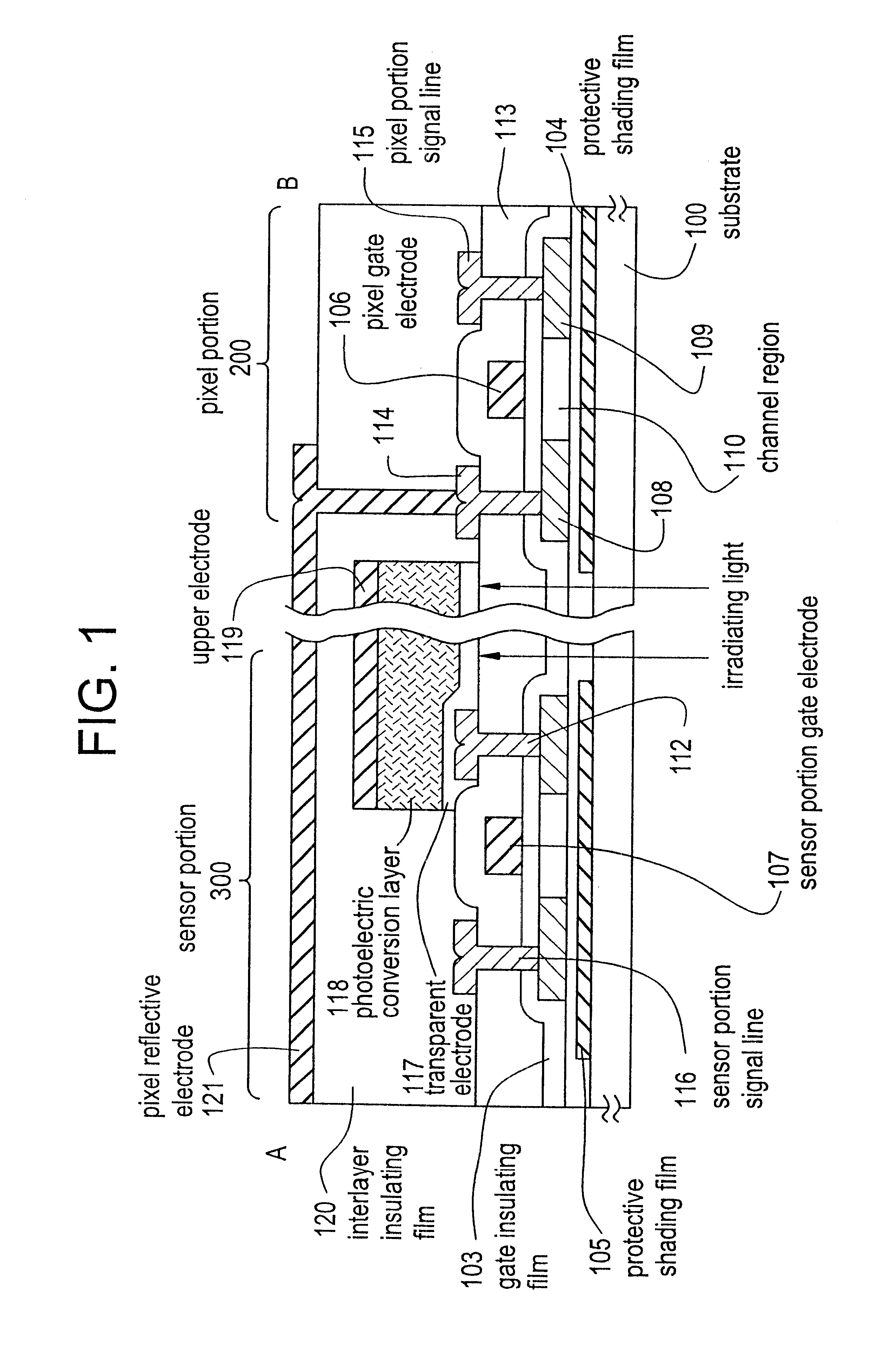
In this embodiment, an example of manufacturing steps of a liquid crystal panel having a sensor portion receiving light from a back surface of a liquid crystal display surface will be described in detail with reference to FIGS. 5A to 5D and FIGS. 6A to 6C.
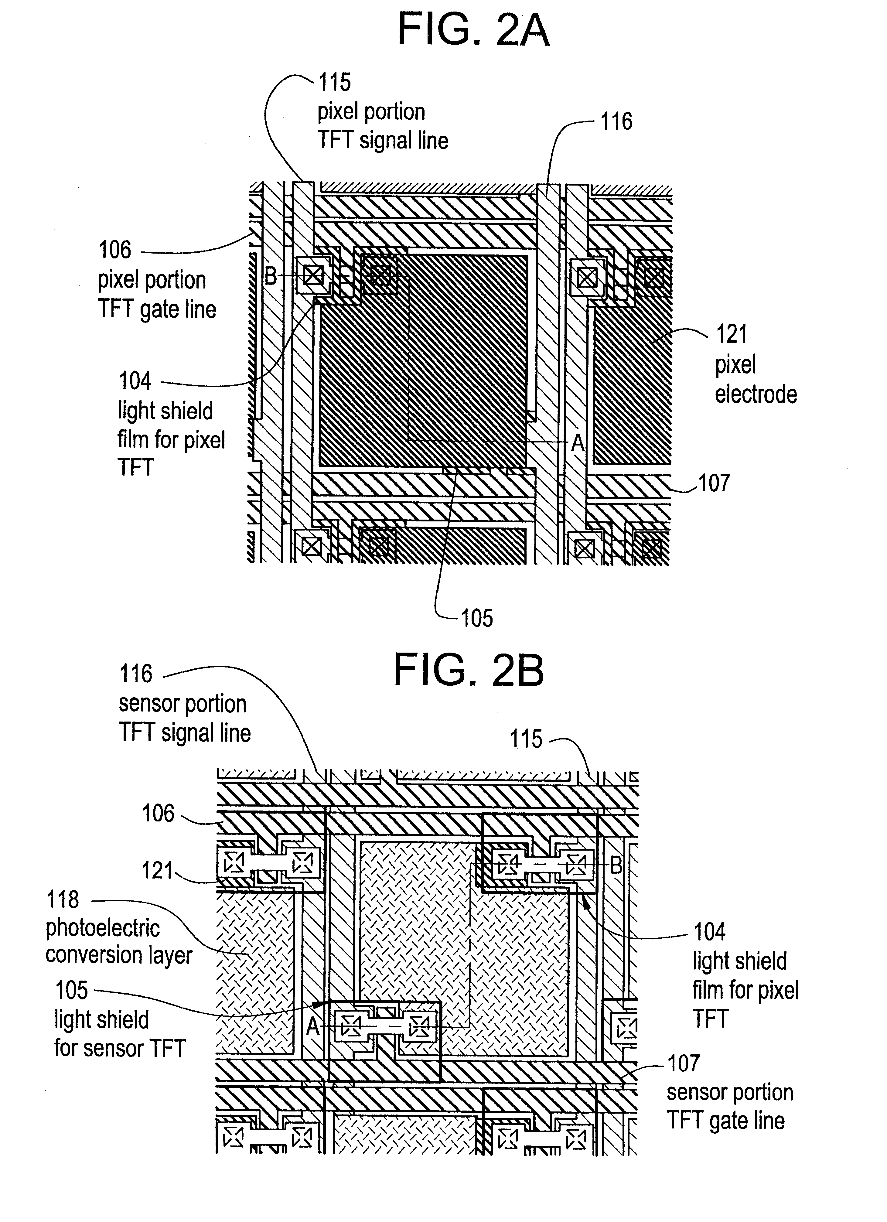
First, an under film 101 is formed on the entire surface of a transparent substrate 100. As the transparent substrate 100, a glass substrate or a quartz substrate having transparency may be used. As the under film, a silicon oxide film with a thickness of 150 nm was formed by a plasma CVD method. In this embodiment, prior to this step of forming the under film, there were provided a shading film 104 for protecting a display pixel portion TFT against light from the back surface, and a shading film 104 for protecting a light receiving sensor portion TFT against light from the back surface. In this embodiment, although the shading films are provided to prevent noise and deterioration, it is not particularly necessary to ...
embodiment 2
[Embodiment 2]
In this embodiment, an example of manufacturing steps of a liquid crystal panel including a sensor portion receiving light from a back surface of a liquid crystal display surface will be described in detail with reference to FIGS. 8A to 8D and FIGS. 9A to 9C.
The feature of this embodiment is that one pixel includes a display pixel portion TFT and a light receiving sensor portion TFT, an interlayer insulating film covering these TFTs are formed, a photoelectric conversion layer is formed on the interlayer insulating film, and is connected to the light receiving sensor portion TFT. Thus, as compared with the embodiment 1, the opening rate is large.
First, an under film 701 is formed on the entire surface of a transparent substrate. A glass substrate or a quartz substrate may be used as a transparent substrate 700. A silicon oxide film with a thickness of 200 nm was formed as the under film by a plasma CVD method. In this embodiment, prior to the step of forming the under ...
embodiment 3
[Embodiment 3]
Although examples in which a non-amplifying image sensor is used, are shown in the embodiments 1 and 2, this embodiment relates to an amplifying type image sensor. More specifically, an example in which an image sensor including semiconductor devices disposed in matrix, will be described.
FIG. 10 is a simplified view of a circuit diagram of a liquid crystal panel using this amplifying type image sensor. The amplifying type image sensor uses three TFTs of a reset transistor T.sub.1, an amplification transistor T.sub.2, and a selection transistor T.sub.3. The most remarkable feature in this circuit diagram is that this diagram includes a reset line 1012, a power source line 1113, a sensor vertical peripheral driving circuit 1009, a sensor horizontal peripheral driving circuit 1008, and a fixed potential line 1115.
Moreover, similarly to the embodiment 1 or 2, the feature of this embodiment is that the wiring line of the liquid crystal display element and the wiring line of...
PUM
| Property | Measurement | Unit |
|---|---|---|
| thickness | aaaaa | aaaaa |
| thickness | aaaaa | aaaaa |
| thickness | aaaaa | aaaaa |
Abstract
Description
Claims
Application Information