Methods of forming thin films by atomic layer deposition

a technology of atomic layer deposition and thin film, which is applied in the direction of coating, chemical vapor deposition coating, metallic material coating process, etc., can solve the problems of difficult control of step coverage, difficult to obtain excellent step coverage, and the possibility of remaining unnecessary atoms in chemical ligand forming reactants

Inactive Publication Date: 2002-10-22
SAMSUNG ELECTRONICS CO LTD
View PDF13 Cites 759 Cited by
  • Summary
  • Abstract
  • Description
  • Claims
  • Application Information

AI Technical Summary

Problems solved by technology

However, it is often difficult to obtain excellent step coverage if a thin film is formed using a conventional chemical vapor deposition (CVD) method or physical vapor deposition (PVD) method.
Particularly, in a conventional CVD method, a dielectric layer having relatively good step coverage can be obtained by a deposition process using a surface kinetic mode, but reactants, which are used in depositing a dielectric layer, are typically conveyed to a substrate so that it is often difficult to control step coverage.
However, if a thin film is formed using these methods, unnecessary atoms contained in a chemical ligand forming reactants may remain within the thin film and become impurities, or create particles on the surface of the substrate.
Accordingly, these deposition processes may require frequent cleaning steps, and may also increase down time in the manufacture of semiconductor devices.
By products, such as NH.sub.4 Cl, may also cause a large quantity of particles to be present during a thin film manufacturing process, and these particles may cause a deterioration in the electric characteristics of the thin film.

Method used


Image

  • Methods of forming thin films by atomic layer deposition
  • Methods of forming thin films by atomic layer deposition
  • Methods of forming thin films by atomic layer deposition

Examples


Embodiment Construction

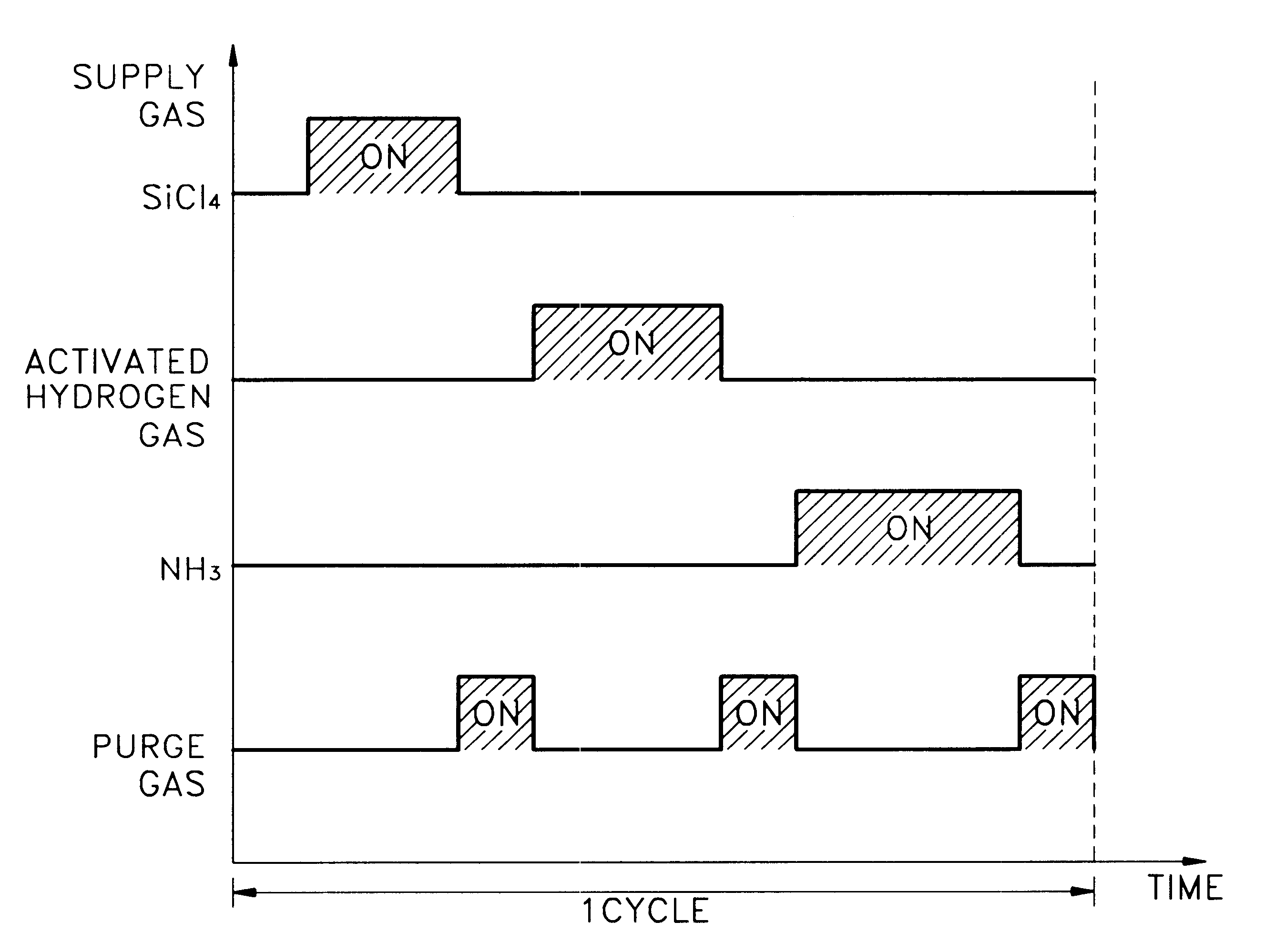
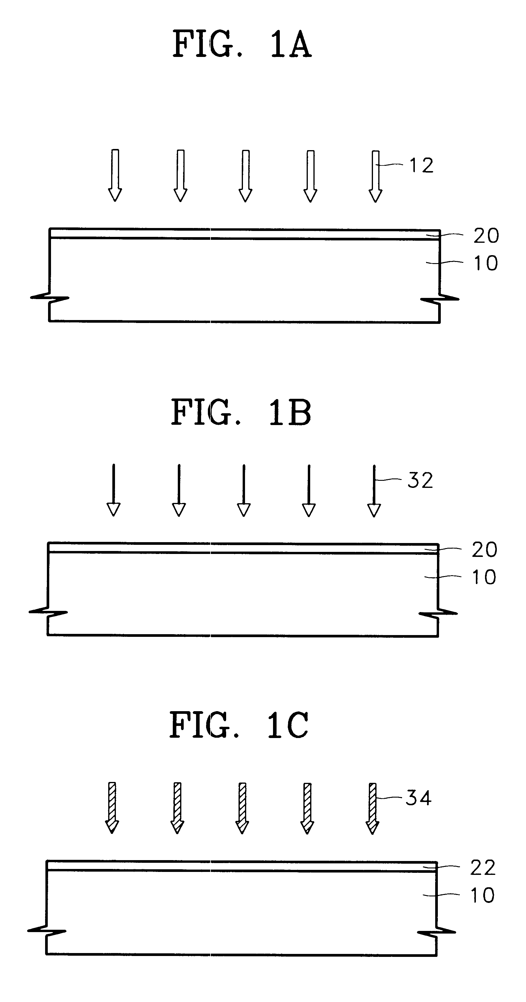
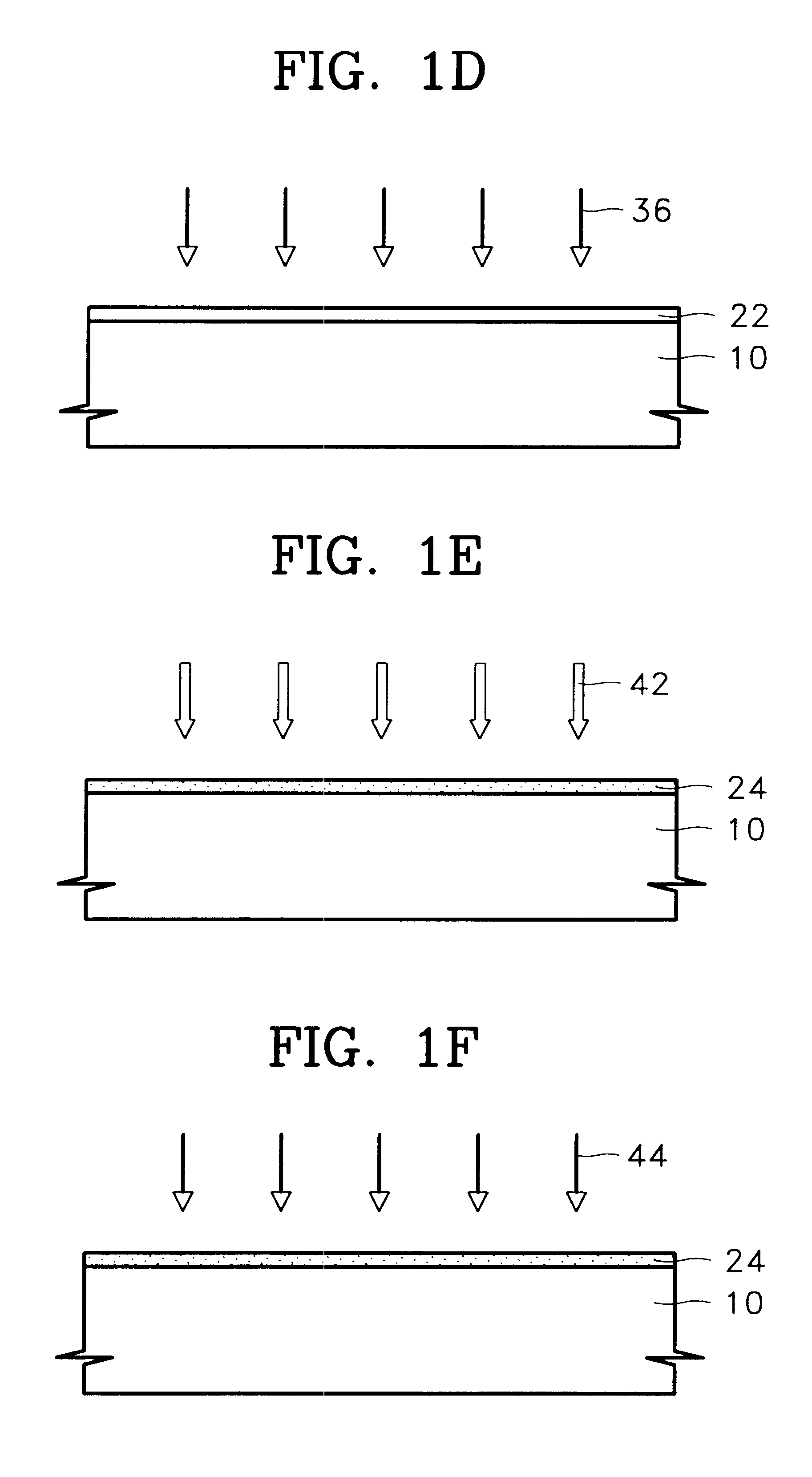
The present invention will now be described more fully hereinafter with reference to the accompanying drawings, in which preferred embodiments of the invention are shown. This invention may, however, be embodied in different forms and should not be construed as limited to the embodiments set forth herein. Rather, these embodiments are provided so that this disclosure will be thorough and complete, and will fully convey the scope of the invention to those skilled in the art. In the drawings, the thickness of layers and regions are exaggerated for clarity. It will also be understood that when a layer is referred to as being "on" another layer or substrate, it can be directly on the other layer or substrate, or intervening layers may also be present. However, when a layer or region is described as being "directly on" another layer or region, no intervening layers or regions are present. Like numbers refer to like elements throughout.

FIGS. 1A through 1F are cross-sectional views illustr...


PUM

PropertyMeasurementUnit
temperatureaaaaaaaaaa

Abstract

Methods of forming thin films include forming a first layer comprising a first element that is chemisorbed to a surface of a substrate, by exposing the surface to a first source gas having molecules therein that comprise the first element and a halogen. A step is then performed to expose the first layer to an activated hydrogen gas so that halogens associated with the first layer become bound to hydrogen provided by the activated hydrogen gas. The first layer may then be converted to a thin film comprising the first element and a second element, by exposing a surface of the first layer to a second source gas having molecules therein that comprise the second element.

Description

This application claims priority to Korean Application No. 2000-73807, filed Dec. 6, 2000, the disclosure of which is hereby incorporated herein by reference.1. Field of the InventionThe present invention relates to methods of manufacturing semiconductor devices, and more particularly, to methods of forming thin films on substrates.2. Background of the InventionA thin film can be used as a dielectric layer of a semiconductor device, a transparent electrical conductor of a liquid crystal display, and a protective layer of an electroluminescent thin film display, for example. In particular, a thin film used as a dielectric layer of a semiconductor device should have limited impurities or defects therein and at the interface of the film in order to ensure high capacitance and limit leakage current. The step coverage and uniformity of a thin film should also be excellent, particularly when used in semiconductor device applications.However, it is often difficult to obtain excellent step ...

Claims


Application Information

Patent Timeline
Patent Type & Authority Patents(United States)
IPC IPC(8): C23C16/40C23C16/34H01L21/02H01L21/318C23C16/44H01L21/20C23C16/455
CPCC23C16/34C23C16/345C23C16/402C23C16/403C23C16/405C23C16/409C23C16/45531C23C16/45542H01L21/3185H01L21/02274H01L21/02194H01L21/02186H01L21/02183H01L21/0228H01L21/02164H01L21/02197H01L21/02178H01L21/20
Inventor LEE, SEUNG-HWANKIM, YEONG-KWANKIM, DONG-CHANPARK, YOUNG-WOOK
Owner SAMSUNG ELECTRONICS CO LTD
Why Eureka
Try Eureka