Circuit board for semiconductor package

a technology of circuit boards and semiconductors, applied in the field of circuit boards, can solve problems such as damage to semiconductor chips or circuit boards, circuit board or semiconductor chips that are susceptible to breakdown, and electrostatic charges accumulated on circuit boards or semiconductor chips,

Inactive Publication Date: 2002-10-22
AMKOR TECH SINGAPORE HLDG PTE LTD
View PDF14 Cites 34 Cited by
  • Summary
  • Abstract
  • Description
  • Claims
  • Application Information

AI Technical Summary

Problems solved by technology

Unfortunately, such semiconductor chips or circuit boards upon which the chips are mounted are susceptible to a breakdown due to electrostatic charges accumulated and discharged during the process for assembling the semiconductor package, e.g., during wire bonding, molding, marking, ball bumping and singulation.
For example, during the encapsulation step, there may be direct friction between a polymer-based encapsulating material and a cover coat or conductive layer of the circuit board (e.g., signaling, grounding and powering circuit patterns) or the semiconductor chip, resulting in electrostatic charges being accumulated on the circuit board or semiconductor chip.
The circuit board with accumulated electrostatic charges is then taken off from a mold for the subs...

Method used


Image

  • Circuit board for semiconductor package
  • Circuit board for semiconductor package
  • Circuit board for semiconductor package

Examples


first embodiment

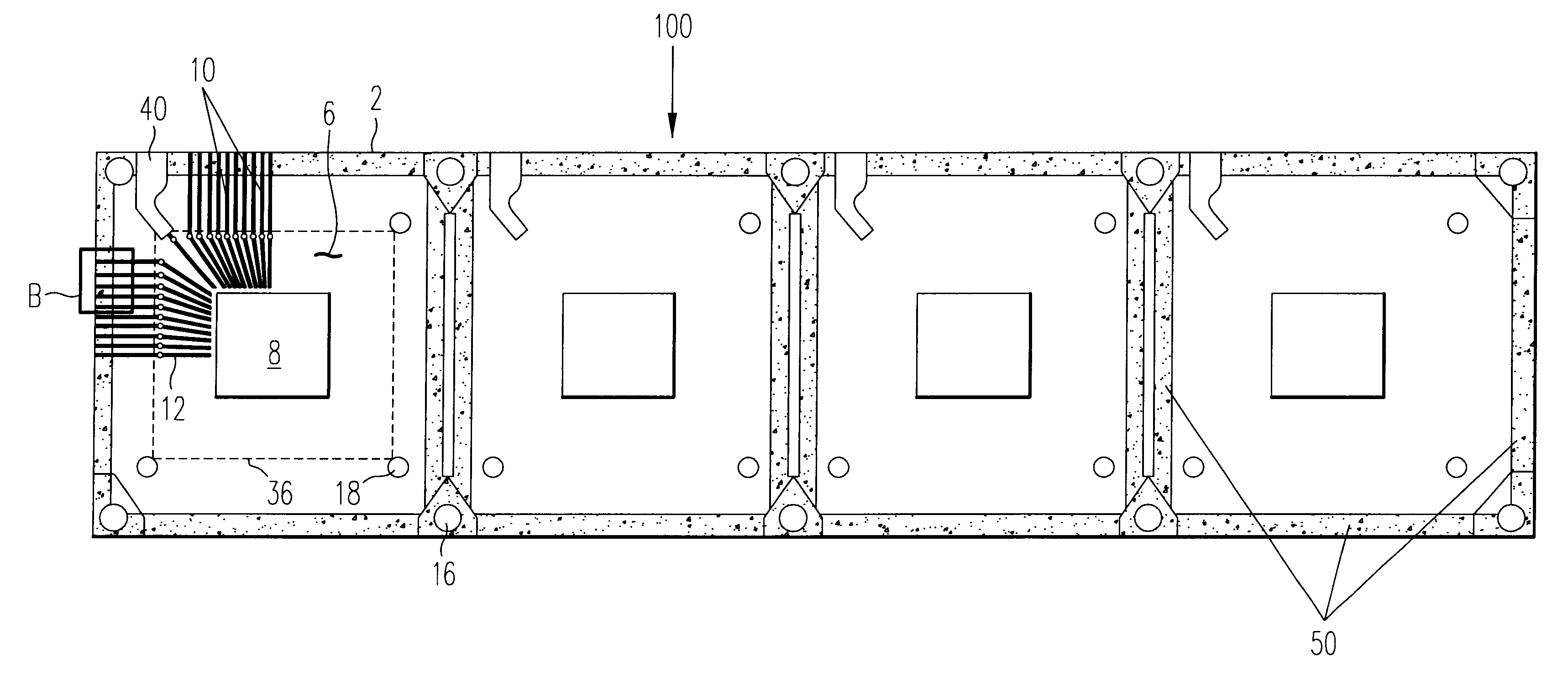
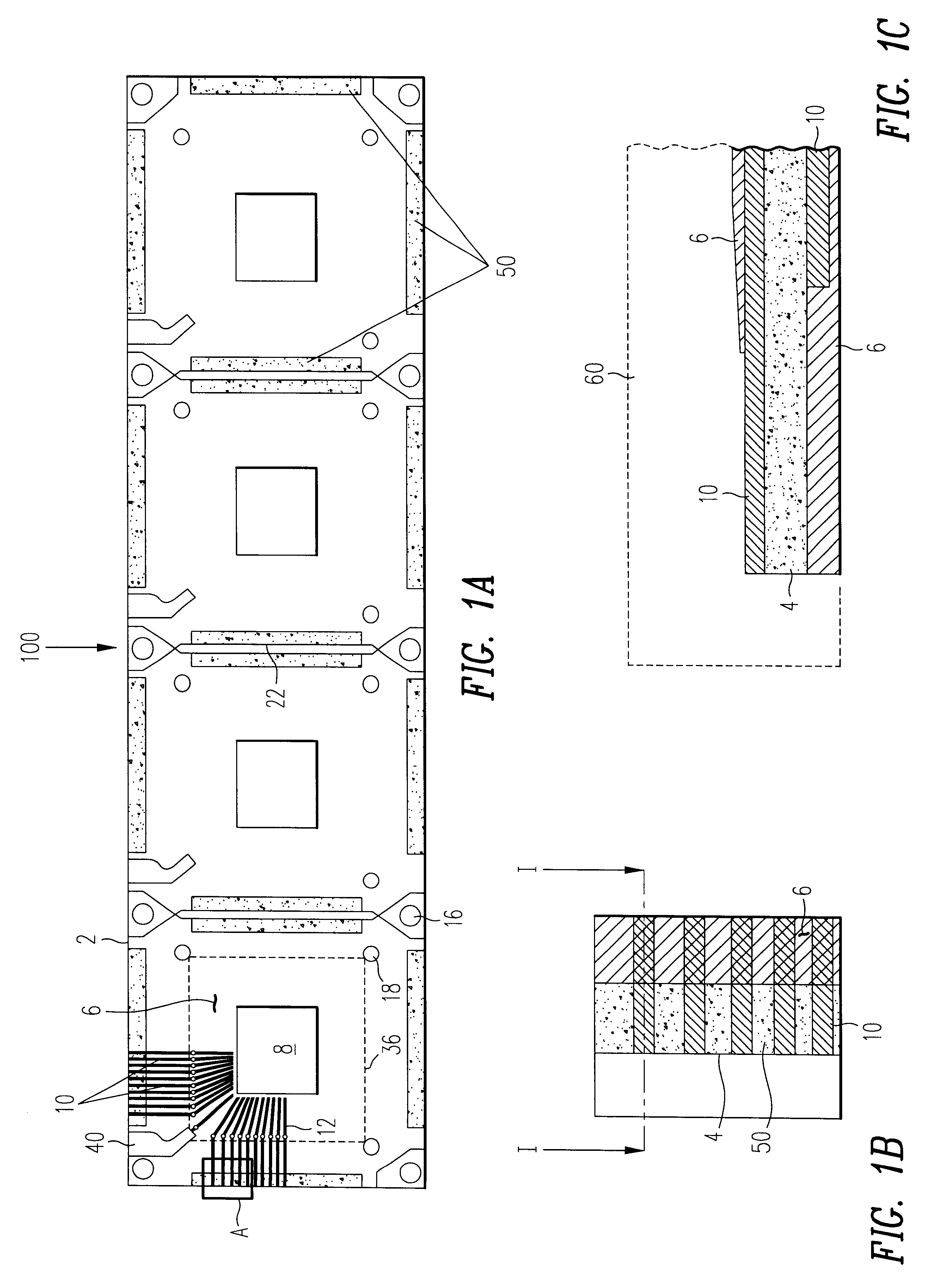
FIG. 1A is a plan view of a circuit board for semiconductor package in accordance with the present invention, FIG. 1B is an enlarged view of part A shown in FIG. 1A, and FIG. 1C is a cross-sectional view taken along the line I--I of FIG. 1B;

A circuit board strip 100 according to the first embodiment of the present invention is essentially analogous to the previously described circuit board strip shown in FIGS. 9A and 9B, with the exception that a cover coat 6 defines opening regions 50 for removing electrostatic charges. Circuit patterns 10 at the periphery of each circuit board unit 2 are exposed through opening regions 50. Opening regions 50 are superimposed over circuit patterns 10 at the outer edges of each circuit board unit 2 and in the vicinity of a slot 22 to be in close grounding contact with a mold 60 in the encapsulating step (FIG. 1C).

That is, the opening regions 50 are provided in the rectangular form at the edge of the individual circuit board unit 2 and in the vicinit...

second embodiment

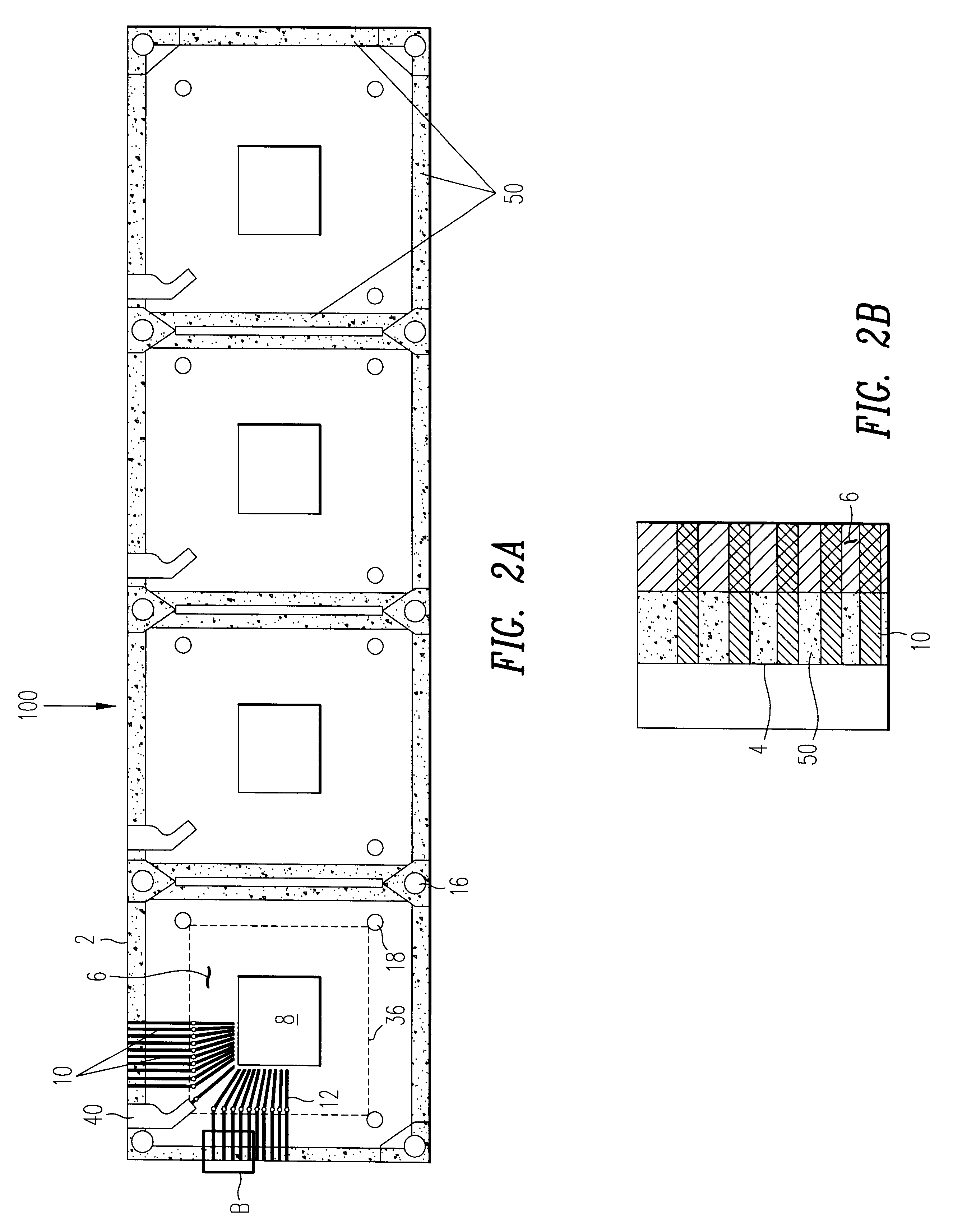
FIG. 3 is a bottom view of the circuit board for semiconductor package in accordance with the present invention.

It is to be noted that the top structure of the circuit board according to the present invention is similar to that of the conventional circuit board and its detailed description will be avoided lest it should obscure the subject matter of the present invention.

The circuit board comprises a plurality of units 2 connected in series with a long vertical slot 22 interposed therebetween, to constitute one strip 100, in which the individual unit 2 has a plurality of singulation holes 18 outside the ball land region 14, and metal lined index holes 16 are disposed in the vicinity of the upper or lower ends of the slot 22 so that fixed pins (not shown) on the corresponding equipment are inserted into the index holes 16 in holding or loading the circuit board strip 100.

As illustrated, the bottom structure of the circuit board according to the present invention has an array of ball ...

third embodiment

FIGS. 5A, 5B, 6A and 6B are bottom and cross-sectional views of a circuit board for semiconductor package in accordance with the present invention.

Centering on resinous substrate 4, a chip mounting region 8 to place a semiconductor chip on is formed on the top surface of the resinous substrate 4, with a plurality of fine signaling, grounding or powering circuit patterns 10 radially arranged at the circumference of the chip mounting region 8 and extending to the edges of the chip mounting region 8. The circuit patterns 10 in the vicinity of the chip mounting region 8 have bond fingers (denoted by no reference numeral). And, the opposite underneath of the resinous substrate 4 is provided with a plurality of ball lands 14 (to be fused to conductive balls). The ball lands 14 on the bottom surface of the resinous substrate 4 are interconnected with the circuit patterns 10 formed on the top surface of the resinous substrate 4 through conductive via holes (not shown). The underneath of the...


PUM


Abstract

A circuit board for semiconductor package is designed to provide a complete grounding with corresponding equipment in the manufacture of the semiconductor package based on a circuit board, thereby preventing a breakdown of the circuit board or semiconductor chip caused by electrostatic charges. The printed circuit board for semiconductor package includes: a resinous substrate; a chip mounting region formed on the top surface of the resinous substrate for mounting a semiconductor chip thereon; a plurality of fine circuit patterns radially disposed in the circumference of the chip mounting region and extending to the edge of the chip mounting region; a plurality of ball lands formed in an array on the bottom surface of the resinous substrate, to be fused to conductive balls; a conductive via hole connecting the circuit patterns on the top surface of the resinous substrate to the ball lands on the bottom surface of the resinous substrate; a cover coat applied to the top and bottom surfaces of the resinous substrate to protect the circuit patterns from an external environment and make the ball lands open to the exterior; and a means for removing electrostatic charges provided at the edge of the substrate and connected to the plural circuit patterns to remove electrostatic charges in the manufacture of semiconductors.

Description

1. Field of the InventionThe present invention relates to a circuit board for a semiconductor a package and, more particularly, to a circuit board for semiconductor package having a structure that completely grounds corresponding equipment used in the manufacture of semiconductor packages based on the circuit board, thereby preventing a breakdown of the semiconductor chip or circuit board due to electrostatic discharge ("ESD").2. Description of the Related ArtGenerally, a circuit board for semiconductor package fixedly supports a semiconductor chip mounted on a main board, and intermediates required electrical signals between the semiconductor chip and the main board. During manufacturing of the package, a plurality of circuit board units are joined in one strip, and the packages are made in parallel. The individual circuit board units usually include an insulative thermosetting resin substrate or film coated with a copper circuit pattern on both sides thereof. Portions of the circu...

Claims


Application Information

Patent Timeline
IPC IPC(8): H05K1/02H05K3/28H05K3/00H01L23/12H01L23/60H01R12/00
CPCH01L23/60H05K1/0259H05K1/0215H05K3/0052H05K3/28H05K2201/09354H01L2924/0002H01L2924/00
Inventor LEE, CHOON HEUNGSHIN, WON DAIKO, CHANG HOONSHIN, WON SUNLEE, SEON GOOLEE, WON KYUNJANG, TAE HOANYANG, JUN YOUNG
Owner AMKOR TECH SINGAPORE HLDG PTE LTD
Why Eureka
Try Eureka