It is an extremely tedious and an error-prone process because of the tight tolerance requirements and the minuteness of the individual components.
Due to the large number of components and the exacting details required by the fabrication process, physical design is not practical without the aid of computers.
Currently available physical design
automation systems are limited in that they are only capable of placing and routing approximately 20,000 devices or cells.
This expedient is not satisfactory since the resulting placement solution is far from optimal.
Layout of the entire circuit cannot be handled due to the limitation of memory space as well as the computation power available.
However it is computationally quite hard.
A particular placement may lead to an unroutable design.
For example, routing may not be possible in the space provided.
This is due to the fact that once the position of each block is fixed, very little can be done to improve the routing and overall
circuit performance.
Due to the nature of the routing algorithms, complete routing of all connections cannot be guaranteed in many cases.
For example, a
poor quality placement cannot be fully cured by high quality routing.
Since placement may produce an unroutable
layout, the
chip might need to be replaced or re-partitioned before another routing is attempted.
The complexity of each step varies depending on the design constraints as well as the design style used.
Thus, the number of possible placements is extremely large.
In the case of a simple pairwise interchange
algorithm, it is possible that a configuration achieved has a cost higher than that of the optimum, but no interchange can cause further cost reduction.
Simulated annealing helps to avoid getting stuck at a local optima by occasionally accepting moves that result in a cost increase.
Moves that result in an increase in cost are accepted with a probability that decreases over the iterations.
The analogy to the actual annealing process is heightened with the use of a parameter called temperature T. This parameter controls the probability of accepting moves that result in increased cost.
However, after doing so, some cells may be duplicated while other cells are deleted.
It must be carefully chosen because while it can introduce more useful genes, most mutations are harmful and reduce fitness.
However, if the individuals are chosen randomly there is no way to
gain improvement from older generation to new generation.
However, attempting to perform genetic
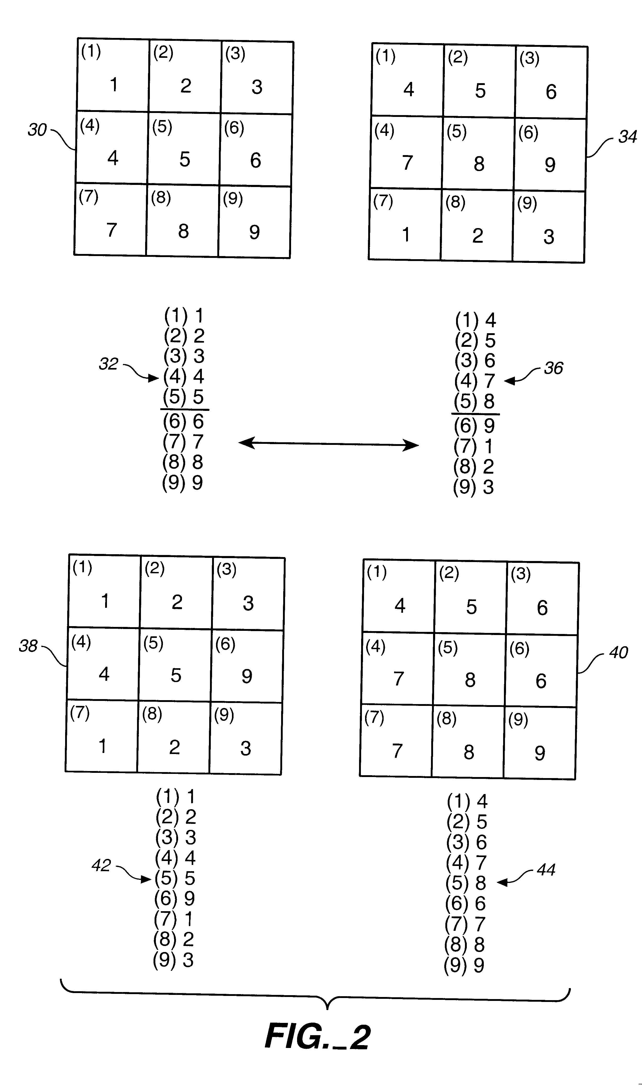
crossover using the conventional representation will result in duplication and / or omission of cells, and other illegal placements.
Both of the exemplary placements are illegal, in that they include duplications and omissions of cells.
It is clear that this method is inapplicable to the physical design of
integrated circuit chips because the circuits would be inoperative if cells were duplicated and / or omitted.
The additional computing time required for the implementation of Shahookar's methods increases the total computer time for a typical
integrated circuit design to such an inordinate value that it would be impractical to implement in a commercial production environment.
However, this is not always the case.
A major factor that prevents conventional algorithms from being utilized for the placement and routing of larger number of cells is that the physical design problem is executed using serial or uniprocessor computers.
Execution of these iterations is extremely
time consuming, requiring days, or even weeks or months to produce a design for a large integrated circuit.
Since this does not occur, a large number of non-optimal solutions are generated, and a human
technician is required to obtain an overview of the process and divert it away from false and / or inefficient solutions.
In applying genetic algorithms and other fitness improvement operations to solving integrated circuit
cell placement and other optimization problems, an important issue is that the computational requirements increase very rapidly with problem size.
The size of the
population required to find the optimum placement also increases with the problem size, so the memory requirements increase very rapidly.
Thus, the computation time increases rapidly with problem size.
Taking the memory requirements and computation time together, the computational requirements increase very rapidly with problem size.
Using this approach to find an optimal placement of a state-of-the-art
chip with 100,000 or more cells is not feasible.
However, the inherent characteristics of the conventional DSM design frustrate the accomplishment of this goal using presently available microelectronic circuit fabrication technology.
The processor that ordered the memory access operation which resulted in the
cache miss is "stalled" during the cache resolution period, and cannot execute any other instructions until the memory access operation is completed.
However, a cache memory of conventional size is too large to fit on a single integrated circuit chip together with a processor, main memory and the requisite logic and control circuitry.
The problem is exacerbated by the fact that cache memory is conventionally implemented as SRAM, whereas main memory is implemented as
DRAM.
The high latency and
cache miss cost for main memory access in a conventional multi-chip DSM
system, even if a large cache memory is provided to reduce the
cache miss rate, reduce the effective
processing speed to such an extent that complicated processors are required to increase the processing speed to an acceptable value.
In addition to being complicated and expensive, such processors are too large to fit on a single integrated circuit chip together with the other elements of a DSM node.
Although effective, communication using these networks is relatively slow, and a complicated and expensive
network interface adapter must be provided for each device that is to be connected to a network.
However, global routing is very
time consuming, and impractical to perform after each
local congestion reduction iteration within the limits of current microelectronic circuit technology.
One processor, for example, can operate at very high speed but be relatively inefficient at handling a variety of input / output protocols, whereas another processor can have the opposite characteristics.
Prior art distributed processing schemes suffer from drawbacks including difficulty in varying the number of processors, failure or crashes of individual processors, and optimal processor utilization in various diversified applications.
If there are tasks that are marked as being assigned but not completed, the possibility exists that one or more of the workers to whom the tasks were assigned had a processor failure, crashed or was
shut down to free the processor for other uses.
Although congestion can be measured accurately by performing at least a global routing after placement, this is extremely
time consuming, and impractical where a very large number of placements must be evaluated.
Assigning non-zero congestion factors to idle cells would produce an erroneously high indication of congestion.
This is necessary because the possible number of placements of N cells is N!, and for an integrated circuit chip including hundreds of thousands of cells N! will be such a huge number that the amount of data representing all of the possible placements could not easily or reasonably be processed using existing
computer technology.
These prior art selection of
mutation methods are limited in effectiveness as they do not address the cost factors of the individual cells in the placements.

