Plasma display device

a display device and plasma technology, applied in the field of cathode ray tubes, can solve the problems of difficult representation, affecting the quality of plasma display, and the inability to control the gradation of display smoothly

Inactive Publication Date: 2002-12-24
LG ELECTRONICS INC
View PDF7 Cites 26 Cited by
  • Summary
  • Abstract
  • Description
  • Claims
  • Application Information

AI Technical Summary

Problems solved by technology

Cathode ray tubes, which have been widely used as image display apparatuses, have bulky construction with large weight and requirements for high supply voltage, and therefore have been replaced by flat panel-shaped image display apparatus such as plasma display device (also referred to as a plasma display panel).
As a result, gradation of display cannot be controlled smoothly for the image of sea having insufficient luminance, resulting in giving a grained impression of the blue sea to viewers.
An im

Method used


Image

  • Plasma display device
  • Plasma display device
  • Plasma display device

Examples


example 1

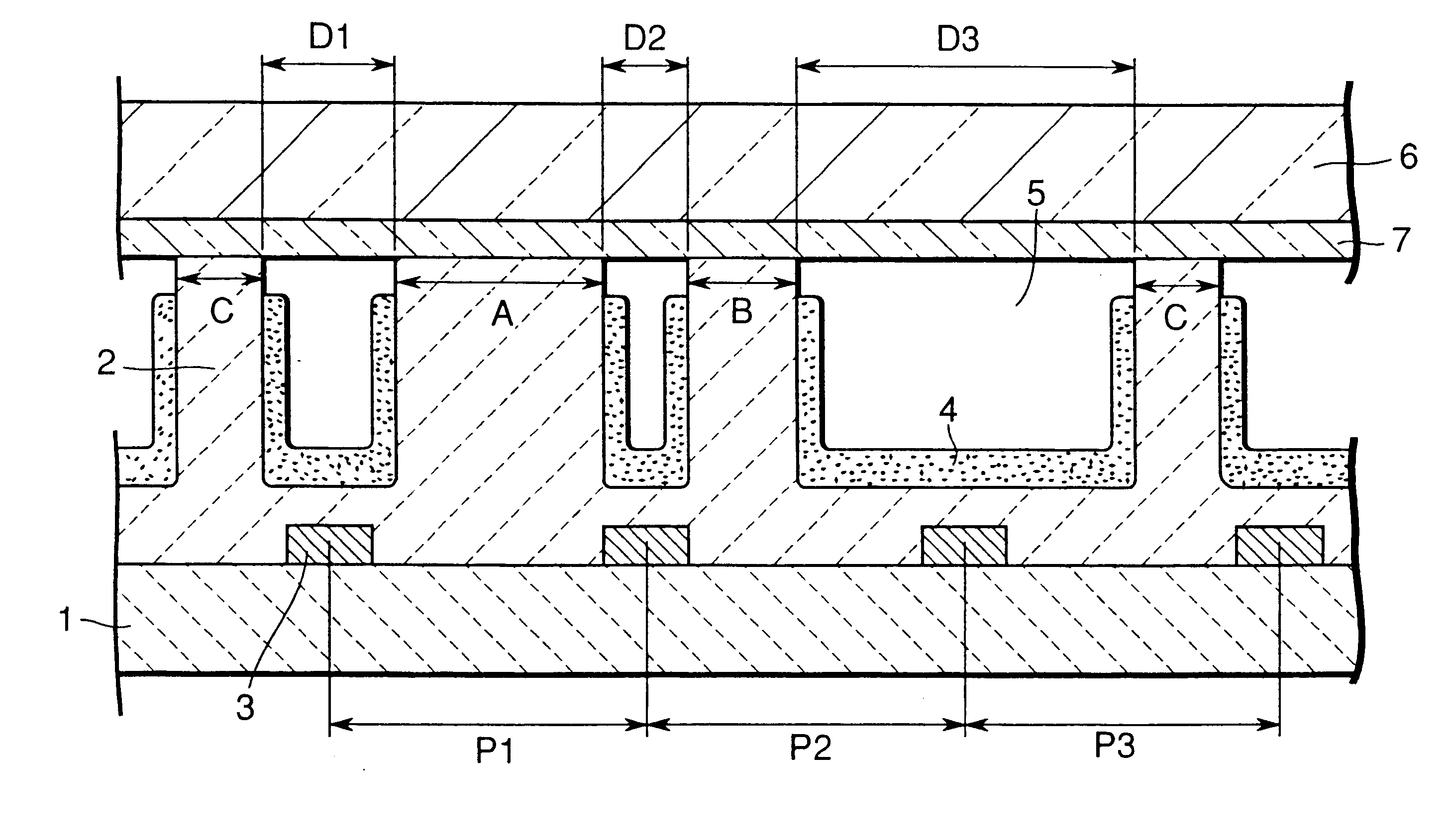
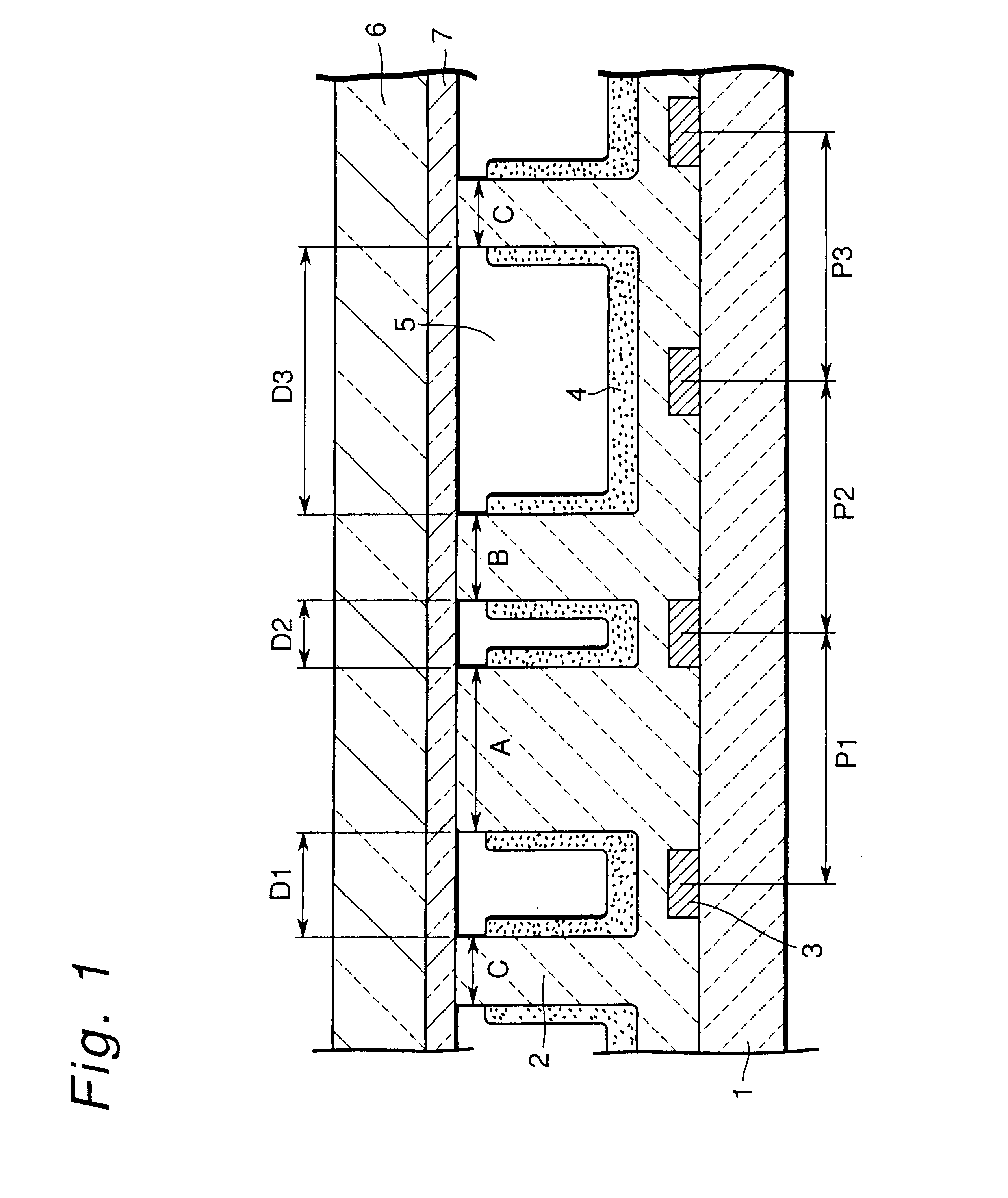
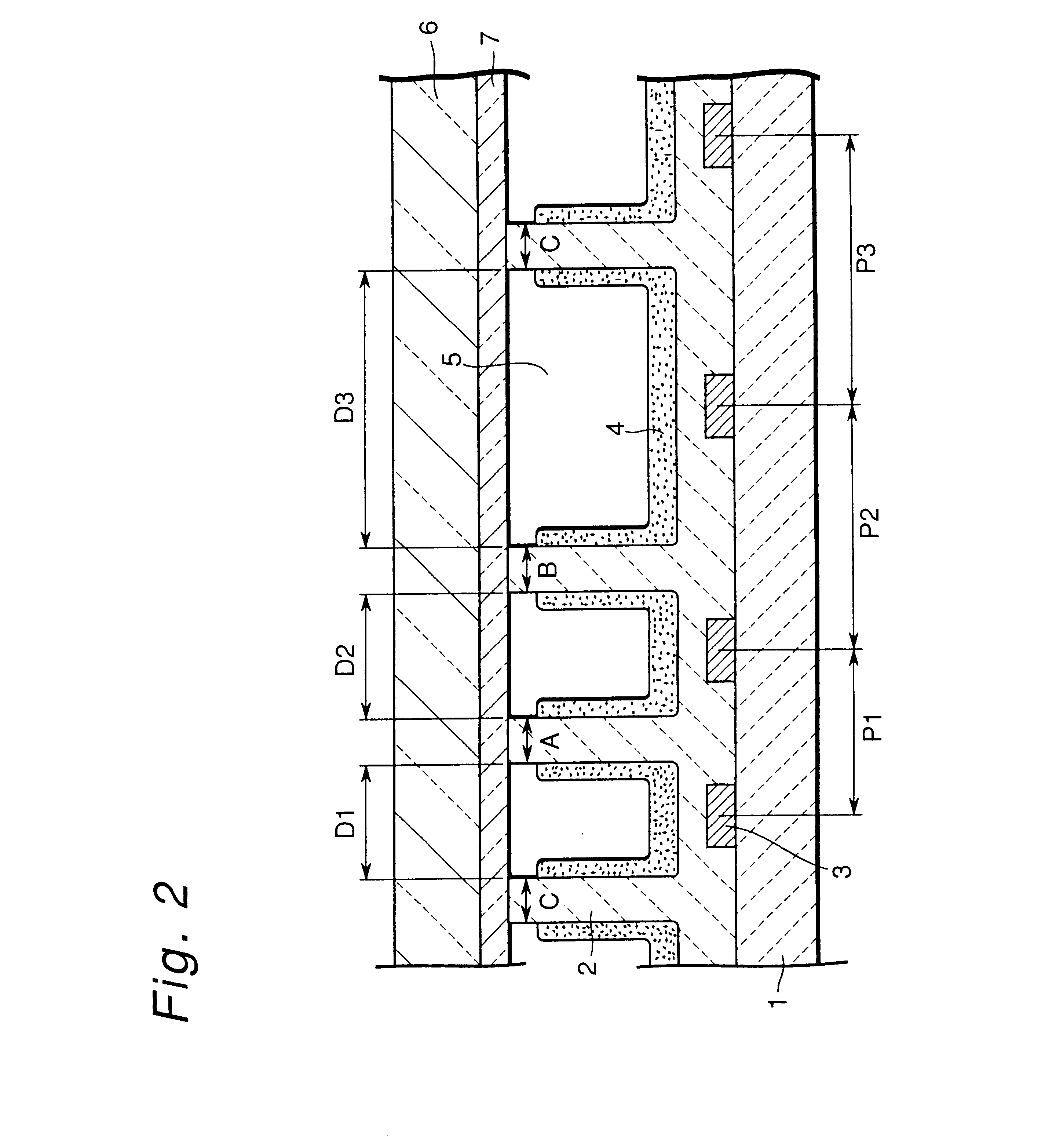
First, the back plate 1 made of soda-lime glass measuring 2 mm in thickness and 30 inches in diagonal size was used. The back plate was coated over the entire surface thereof with an electrode paste including silver as a major component by thick film printing method in the form of stripes 90 .mu.m in width with a pitch of 360 .mu.m, followed by baking, thereby to form address electrodes 3.

The address electrodes 3 are aligned and the partition walls 2 measuring 25 .mu.m in width and 150 .mu.m in height are formed by pressing the die, dried and fired.

In the cases to be described below, first a monochromatic plasma display panel was produced. Only a past including a fluorescent substance, mixture of (Y,Gd)BO.sub.3 to Mn oxide, for red color, was applied to all the light emitting cells on the back plate of the plasma panel by screen printing method, thereby to fire a red fluorescent substance layer 4. Then the front plate 6 with the discharge electrode 7 was integrated and filled with a...

example 2

Similarly to the example 1, the values of luminance of the individual fluorescent substances were measured, with the luminance data being used to determine the widths of the light emitting cells 5 of the fluorescent substances as 325 .mu.m for D1 (red), 250 .mu.m for D2 (green) and 430 .mu.m for D3 (blue), so that the product of the luminance of the individual fluorescent substance and the cube-of the light emitting cell width is substantially constant.

The die was designed using the calculated value of the light emitting cell width as the base, and the plasma display device shown in FIG. 2 was made as described below. The back plate made of soda-lime glass measuring 2 mm in thickness and 30 inches in diagonal size was coated with an electrode paste including silver as a major component by thick film printing method in the form of stripes 90 .mu.m in width in order to form the address electrode 3. In this example, stripes were formed at a pitch of P1=315 .mu.m between red and green, ...


PUM


Abstract

In a plasma display device comprising a pair of opposing insulating substrates and a plurality of light emitting cells 5 formed from partition walls which divide the space between the insulating substrates while a plurality of electrodes are formed in the light emitting cells 5 and the inner space is filled with a discharge gas and plasma being generated by applying a voltage selectively between the electrodes so that the fluorescent substances 4 formed on the inner walls of the light emitting cells emit light as light emitting elements, wherein sizes of the light emitting cells 5 of different colors are made different according to the luminance of the fluorescent substance of the corresponding color. That is, cells which emit light of a color of luminance lower than the other cells are made with larger opening to obtain equally high luminance for all the three primary colors, thereby mitigating the deviation in the luminance among the fluorescent substances and achieving full-color display of high image quality with high color purity.

Description

The present invention relates to a plasma display device used for colored image display of high brightness having low weight and thin construction.PRIOR ARTCathode ray tubes, which have been widely used as image display apparatuses, have bulky construction with large weight and requirements for high supply voltage, and therefore have been replaced by flat panel-shaped image display apparatus such as plasma display device (also referred to as a plasma display panel). The plasma display devices have been developed as the multimedia and telecommunication technologies advance and have been finding new, expanding applications.The plasma display device is considered to be a promising colored image display apparatus in the future, because it has high image quality achieved by the use of plasma light emission, availability for large screen size and thin and low weight construction without occupying much place to be installed.A plasma display device, as shown in FIG. 4, has such a constructi...

Claims


Application Information

Patent Timeline
IPC IPC(8): H01J17/49H01J11/12H01J11/22H01J11/26H01J11/34H01J11/36H01J11/42H01J17/04
CPCH01J11/12H01J11/36H01J11/42
Inventor SAKAI, HISAMITSUKATO, MASASHIMAEDA, TETSUYAWATADA, KAZUOHATANAKA, JUNJI
Owner LG ELECTRONICS INC
Why Eureka
Try Eureka