Polishing pad conditioning system

a conditioning system and polishing pad technology, applied in the direction of abrasive surface conditioning devices, manufacturing tools, lapping machines, etc., can solve the problems of reducing the removal or polishing rate and repeatability, affecting the device performance, and not always removing waste from the flushing process

Inactive Publication Date: 2003-01-21
BENNER ROBERT LYLE +2
View PDF7 Cites 97 Cited by
  • Summary
  • Abstract
  • Description
  • Claims
  • Application Information

AI Technical Summary

Problems solved by technology

This type of flushing does not always remove the waste.
These materials reduce removal or polishing rates and repeatability and can produce defects in the form of scratches that damage the wafer surface and device performance (opens, shorts).
The CMP process has been reported to be a major source of this contamination.
The uncontrolled delivery and removal (flushing) of process fluids can also cause polishing waste to build-up on many surfaces within the tooling.
When dislodged, these dried / agglomerated compounds can lead to additional defects.
Slurry has proven to be "unstable" prone to agglomeration due to shear forces in delivery systems, heat, and age effects.
There is also potential for diamond particles to fracture or be torn from the metal matrix of the end effector disk and scratch the wafer surface.
This is a very uncontrolled method of removal because the flushing cannot breakup the static layer of slurry on the pad surface nor is it able to dislodge the slurry in the holes of the pad.
This could lead to additional agglomerates of slurry becoming deposited in holes and recesses of the pad.
This slurry can be dislodged, at a later time, and damage subsequent wafers.
The reliance of centrifugal force to present new slurry to the wafer / pad interface is also less controlled or repeatable than required causing variation in removal rates and uniformity.
Additionally, oxidizing slurries sometimes used in this process contribute to the contamination of the pad by interacting with metals that come in close proximity to the pad causing potential contamination of the wafer.
Very often this compression will change the properties of the pad.
In addition, the limited number of points limits the area of pad that has the desired grooves.
This process does nothing to control delivery or removal of process fluid streams, nor active cleaning of the pad.
This saves on costly slurry, the volume of UPW and the expensive waste disposal.

Method used


Image

  • Polishing pad conditioning system
  • Polishing pad conditioning system
  • Polishing pad conditioning system

Examples


Embodiment Construction

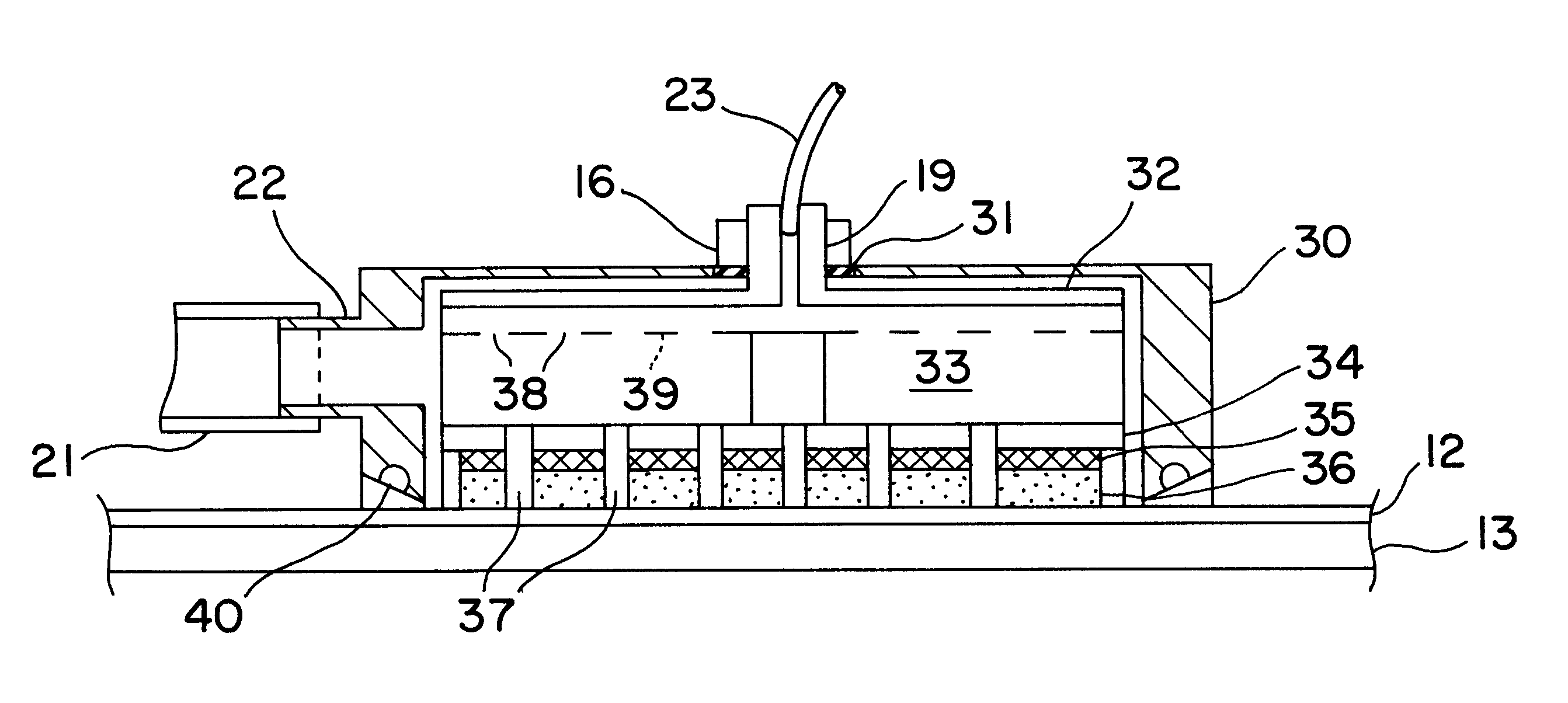
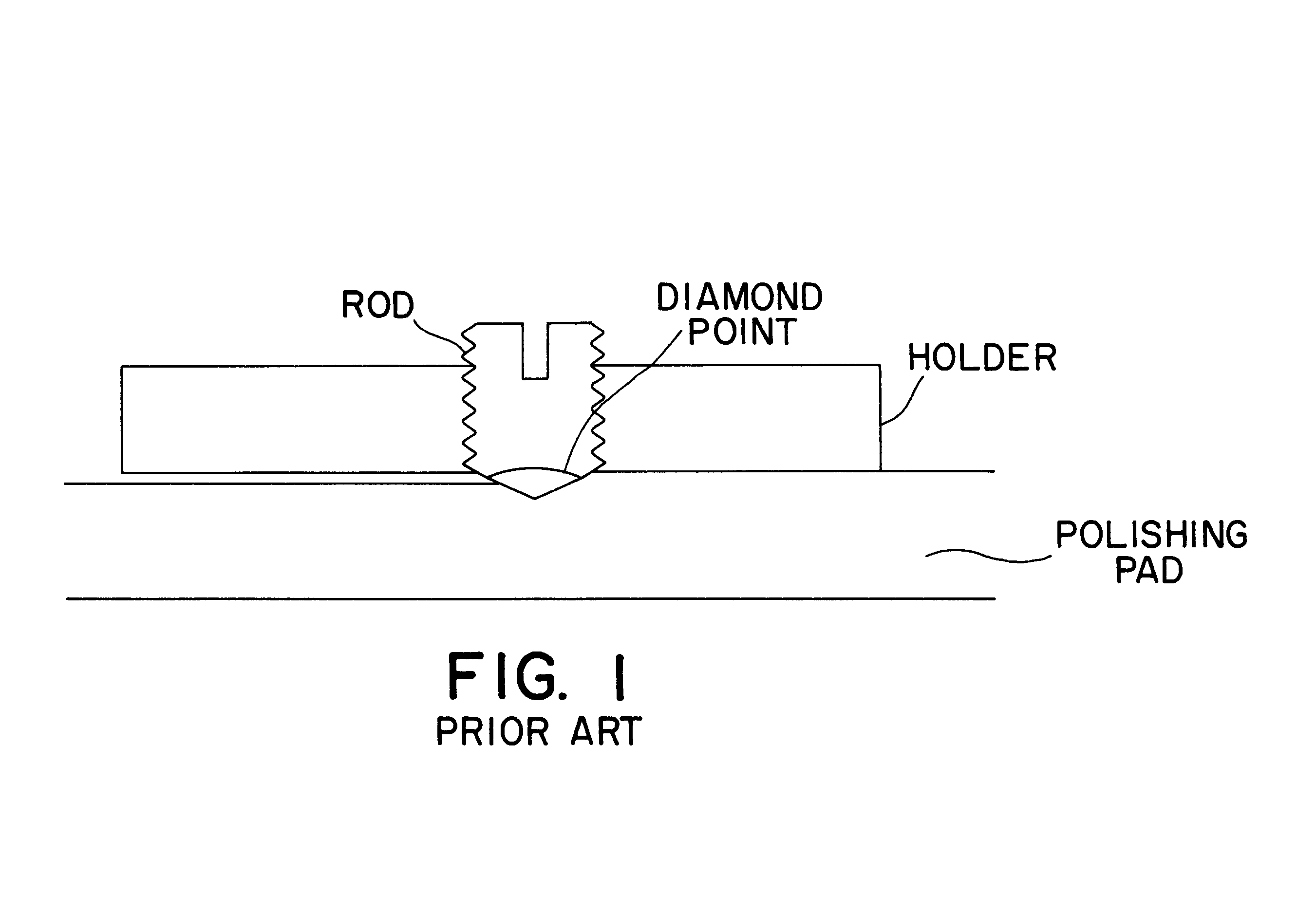
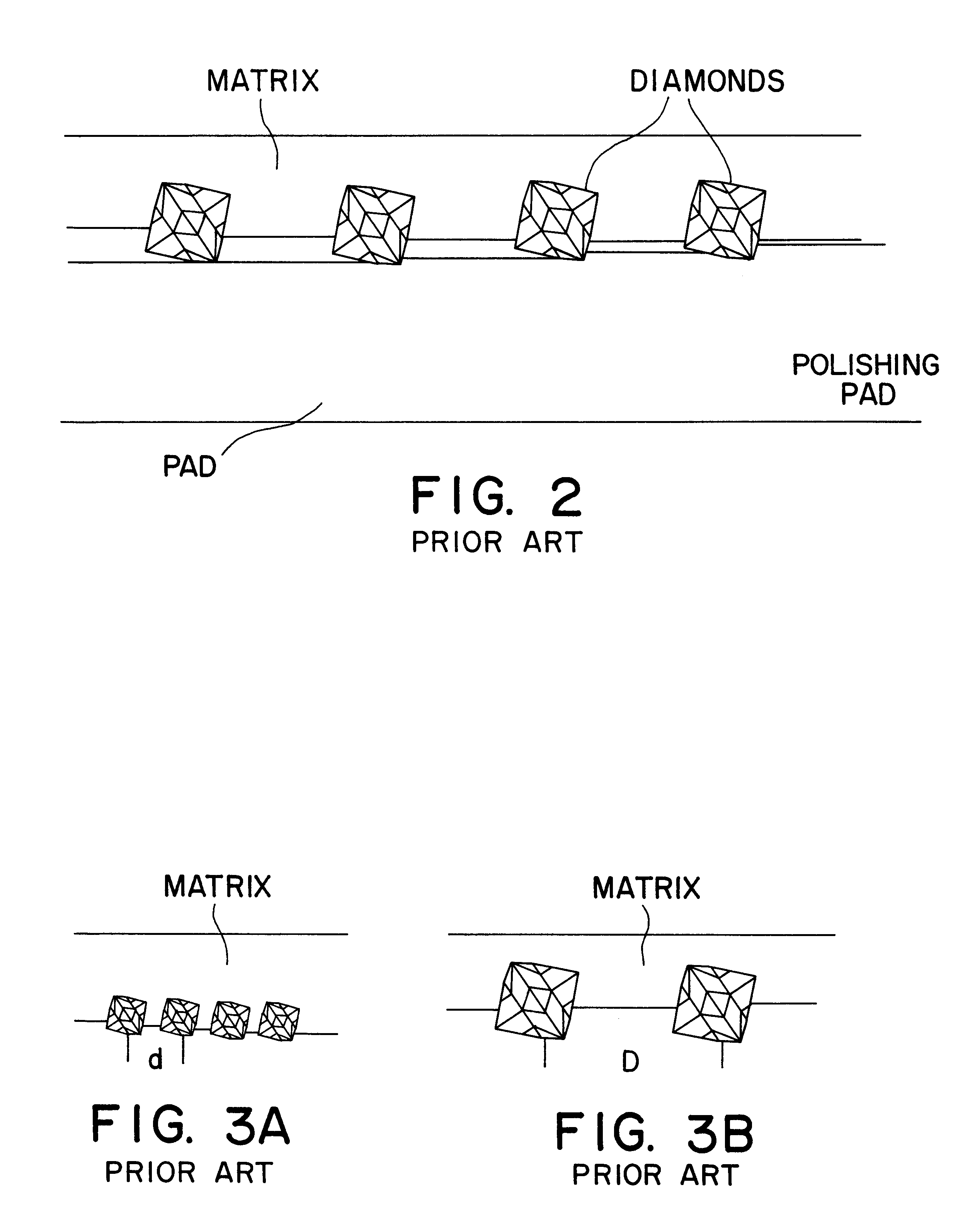
The present invention is an improved apparatus and method for conditioning polishing pads such as those used in Chemical Mechanical Polishing or Planarizing (CMP) Systems for removing irregularities on semiconductor wafer substrates. The specific details of the preferred embodiment provide a thorough understanding of the invention, however, some CMP system elements which operate in conjunction with the present invention have not been elaborated on because they are well known and may tend to obscure other aspects that are unique to this invention. It will be obvious to one skilled in the art that the present invention may be practiced without these other system elements.

Referring to FIG. 4, a perspective view of a typical CMP system 10 is illustrated generally comprising a polishing head (not shown) that applies pressure to wafer 11 against a polishing pad 12 through a wafer carrier and support arm (not shown), and a polishing pad conditioning apparatus 15. Wafer 11 is rotated on pol...


PUM

PropertyMeasurementUnit
thicknessaaaaaaaaaa
diameteraaaaaaaaaa
diameteraaaaaaaaaa

Abstract

A system for conditioning rotatable polishing pads used to planarize and polish surfaces of thin film integrated circuits deposited on semiconductor wafer substrates, microelectronic, and optical system. The system has a pad conditioning apparatus, process fluids, a vacuum capability to pull waste material out of the conditioning pad, self-contained flushing means, and a piezo-electric device for vibrating the pad conditioning apparatus.

Description

1. Field of the InventionThe present invention relates to the field of semiconductor fabrication, microelectromechanical systems (MEMS) fabrication or precision polishing; more specifically to apparatuses and methods for Chemical Mechanical Polishing (CMP) and planarization.2. Description of Related Art W / R to Semiconductor FabricationAn integrated circuit generally consists of a silicon wafer substrate typically produced on fabricated as a disc with a diameter of 100 to 300 millimeters and a thickness of 16 to 40 mils. Metallic dielectric and insulator depositions forming interconnected circuits are created on a wafer by a series of processes (lithography, vapor deposition, oxydation) producing the desired electrical circuitry. An electrical insulating layer, up to one-micron in thickness, is then deposited over the electrical circuit layer. With each layer, a multiplicity of undesired irregularities occur on the surface. These irregularities are on the order of 0.1 to 0.5 microns ...

Claims


Application Information

Patent Timeline
Patent Type & Authority Patents(United States)
IPC IPC(8): B24B53/00B24B53/095B24B53/007B24B37/04B24B53/017
CPCB24B53/095B24B53/017
Inventor BENNER, ROBERT LYLEBENNER, STEPHEN J.BENNER, ROBERT L.
Owner BENNER ROBERT LYLE
Why Eureka
Try Eureka