Semiconductor light-emitting device, electrode for the device, method for fabricating the electrode, LED lamp using the device, and light source using the LED lamp
- Summary
- Abstract
- Description
- Claims
- Application Information
AI Technical Summary
Benefits of technology
Problems solved by technology
Method used
Image

Examples
first embodiment
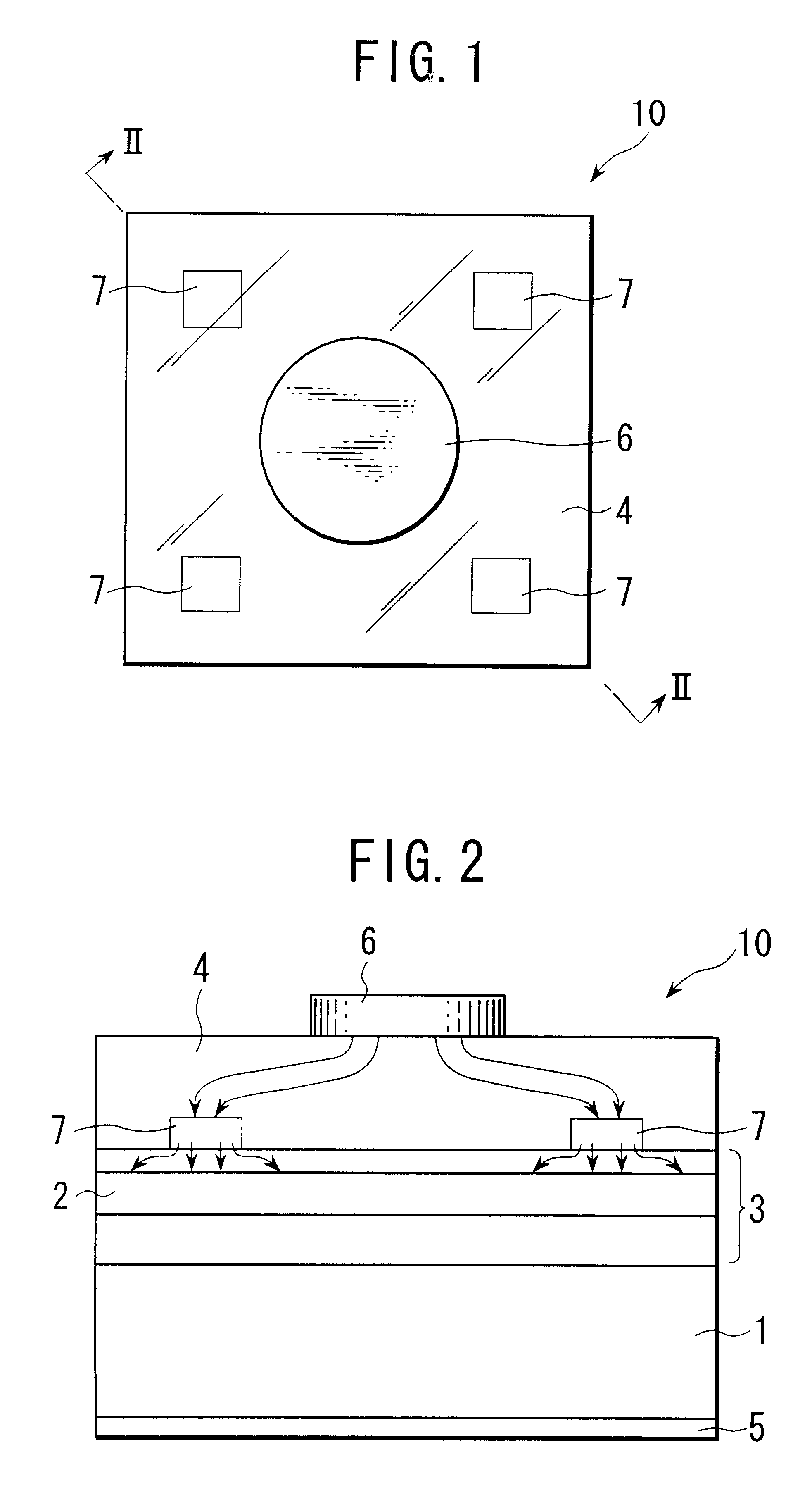
The V.sub.f value (per 20 mA) of the sample device was about 2V, which was approximately equal to the V.sub.f value of the semiconductor light-emitting device 20 of the In the sample device, since the flat ohmic electrode having the total thickness of about 100 nm was provided directly on the upper clad layer 233, the light emission occurred only just below and around the ohmic electrode. A large amount of the emitted light was intercepted by the electrode and could not be taken out. As a result, the light emission intensity of the sample device was at a low level of about 20 mcd.
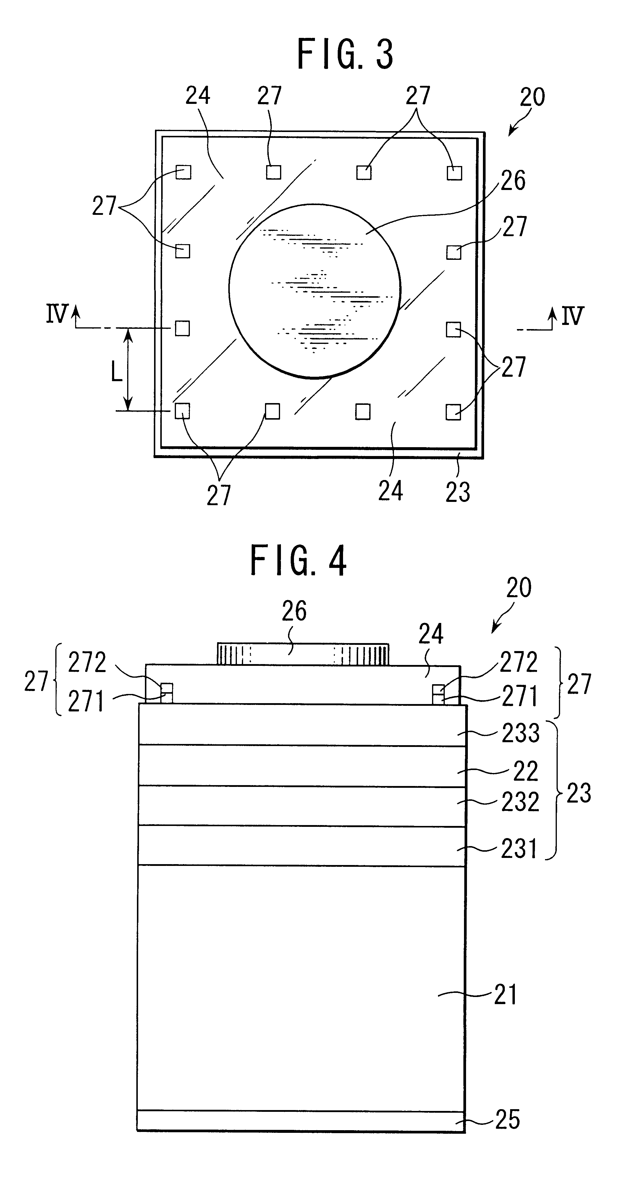
The semiconductor light-emitting device 20 of the first embodiment has a structure in which the ohmic dispersed electrodes 27 whose area of contact with the semiconductor layer 23 (the upper clad layer 233) is small are disposed without reducing the effective light-emitting area S and increasing the V.sub.f value. It is apparent that this structure enables high luminance to be realized.
second embodiment
FIGS. 5 and 6 show the semiconductor light-emitting device according to the present invention. FIG. 5 is a plan view of thereof and FIG. 6 is a cross section taken along line VI--VI in FIG. 5. In these figures, the semiconductor light-emitting device 30 is a light emitting diode (LED) which emits reddish-orange light. The semiconductor light-emitting device 30 is constituted by sequentially stacking on a single crystal substrate 31 of Si-doped n-type (001) 2.degree.-off GaAs, a buffer layer 331 of Si-doped n-type GaAs, a Bragg reflection (DBR) layer 332 of a periodic structure in which 10 Si-doped n-type Al.sub.0.40 Ga.sub.0.60 As layers and 10 n-type Al.sub.0.95 Ga.sub.0.05 As layers are alternately stacked periodically, a lower clad layer 333 of Si-doped n-type (Al.sub.0.7 Ga.sub.0.3).sub.0.5 In.sub.0.5 P, a light-emitting layer 32 made of a mixed crystal of undoped n-type (Al.sub.0.2 Ga.sub.0.8).sub.0.5 In.sub.0.5 P, and an upper clad layer 334 of Mg-doped p-type (Al.sub.0.7 Ga.s...
third embodiment
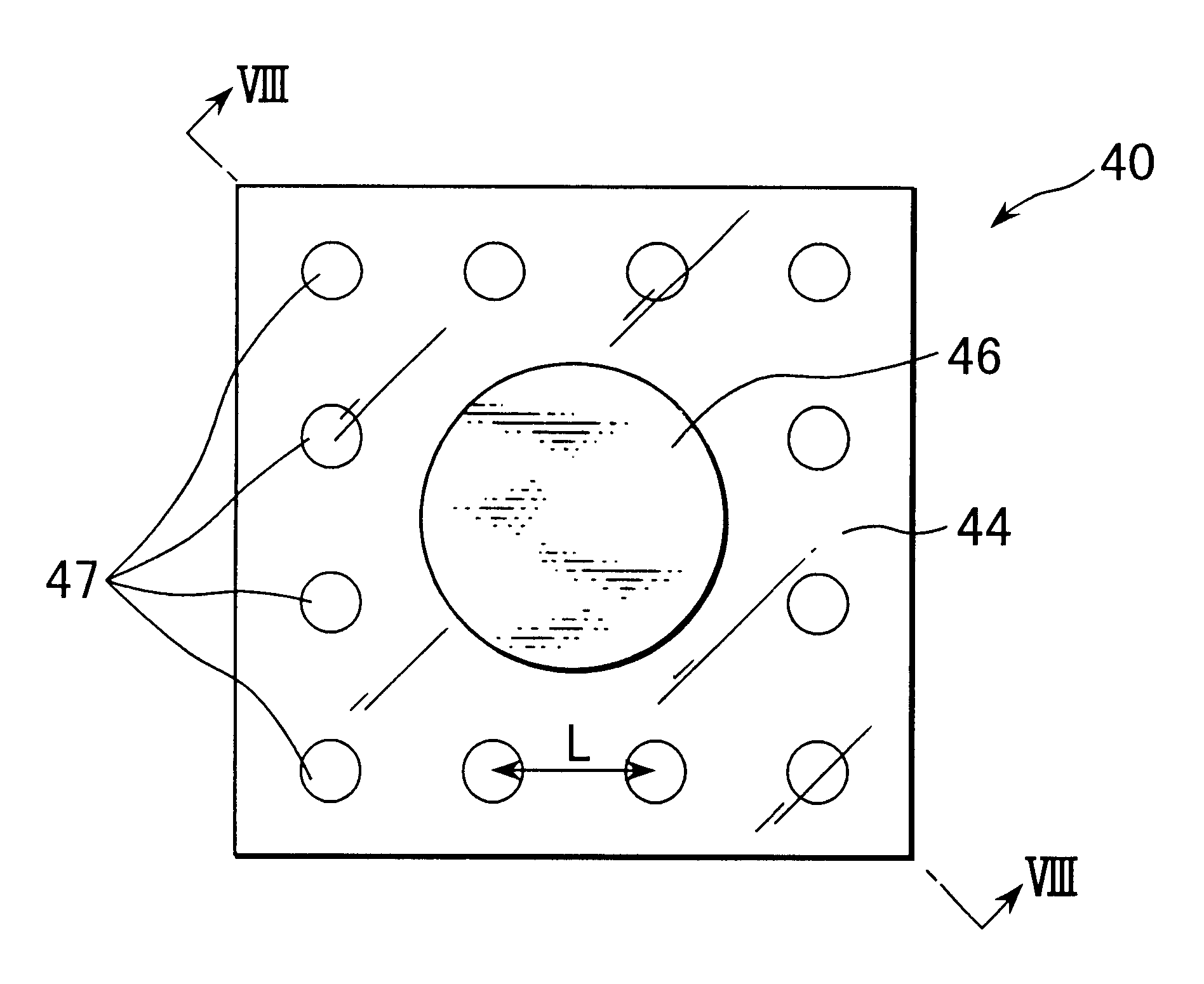
FIGS. 7 and 8 show the semiconductor light-emitting device according to the present invention. FIG. 7 is a plan view thereof and FIG. 8 is a cross section taken along line VIII--VIII in FIG. 7. In these figures, the semiconductor light-emitting device 40 is a light emitting diode (LED) which emits yellowish-green light. The semiconductor light-emitting device 40 comprises a single crystal substrate 41 of Zn-doped p-type (001) 4.degree.-off GaAs and a semiconductor layer 43 formed on the substrate. The semiconductor layer 43 comprises a buffer layer 431 of Zn-doped p-type GaAs, a Bragg reflection (DBR) layer 432 of a structure in which 12 Al.sub.0.4 Ga.sub.0.6 As layers and 12 Al.sub.0.9 Ga.sub.0.1 As layers are alternately stacked, a lower clad layer 433 of Zn-doped p-type Al.sub.0.5 In.sub.0.5 P, a light-emitting layer 42 made of a mixed crystal of undoped (Al.sub.0.4 Ga.sub.0.6).sub.0.5 In.sub.0.5 P, an upper clad layer 434 made of a mixed crystal of Se-doped n-type Al.sub.0.5 In....
PUM
 Abstract
Description
Claims
Application Information