Semiconductor integrated circuit device having an internal voltage generating circuit layout easily adaptable to change in specification

a technology of integrated circuits and circuits, which is applied in semiconductor devices, digital storage, instruments, etc., can solve problems such as insufficient assurance of stable operation, noise, and complicated design

Inactive Publication Date: 2003-02-11
RENESAS ELECTRONICS CORP
View PDF6 Cites 83 Cited by
  • Summary
  • Abstract
  • Description
  • Claims
  • Application Information

AI Technical Summary

Problems solved by technology

Therefore, the signal lines transmitting the reference current and the reference voltage are driven by small driving capabilities, and therefore are susceptible to noises applied from other signal lines or the substrate.
For verifying the layout of the above internal voltage generating circuitry, EDA tools such as layout reference check (DRC: Design Rule Check) usually performed and match verification (LVS: Layout Versus Schematic) between schema (logical description of layout) and layout are employed, but stable operations are insufficiently ensured in many cases.
This complicates the design, and impedes reduction in layout period.
If the storage capacity is small, the voltage generator having the current drive capability exceeding the necessary capability may be used, leading to a problem that an unnecessarily large current is consumed.
This results in a large loss of area.
In the prior art, these changes in structure require restructuring of the floor plan of the power supply circuit, e.g., through the power supply line and cell arrangements, and therefore increase a time required for chip restructuring.
However, these changes in structure occur only to a limited extent and only by integer times in many cases.
In view of stability of the whole operation of the power supply circuit, it is not desirable to change the relative internal arrangement and on-chip positions of the components (MOS transistors) of the reference voltage generating circuit 1 generating such noise-sensitive signals, because such change may impede a noise immunity.
Further, a stabilizing capacitor of a large capacitance value occurs parasitically on each voltage node in these circuits, and the potential change during operation of the circuitry is small (e.g., PN junction between the well and the substrate in the substrate region of the memory array has an extremely...

Method used


Image

  • Semiconductor integrated circuit device having an internal voltage generating circuit layout easily adaptable to change in specification
  • Semiconductor integrated circuit device having an internal voltage generating circuit layout easily adaptable to change in specification
  • Semiconductor integrated circuit device having an internal voltage generating circuit layout easily adaptable to change in specification

Examples


Embodiment Construction

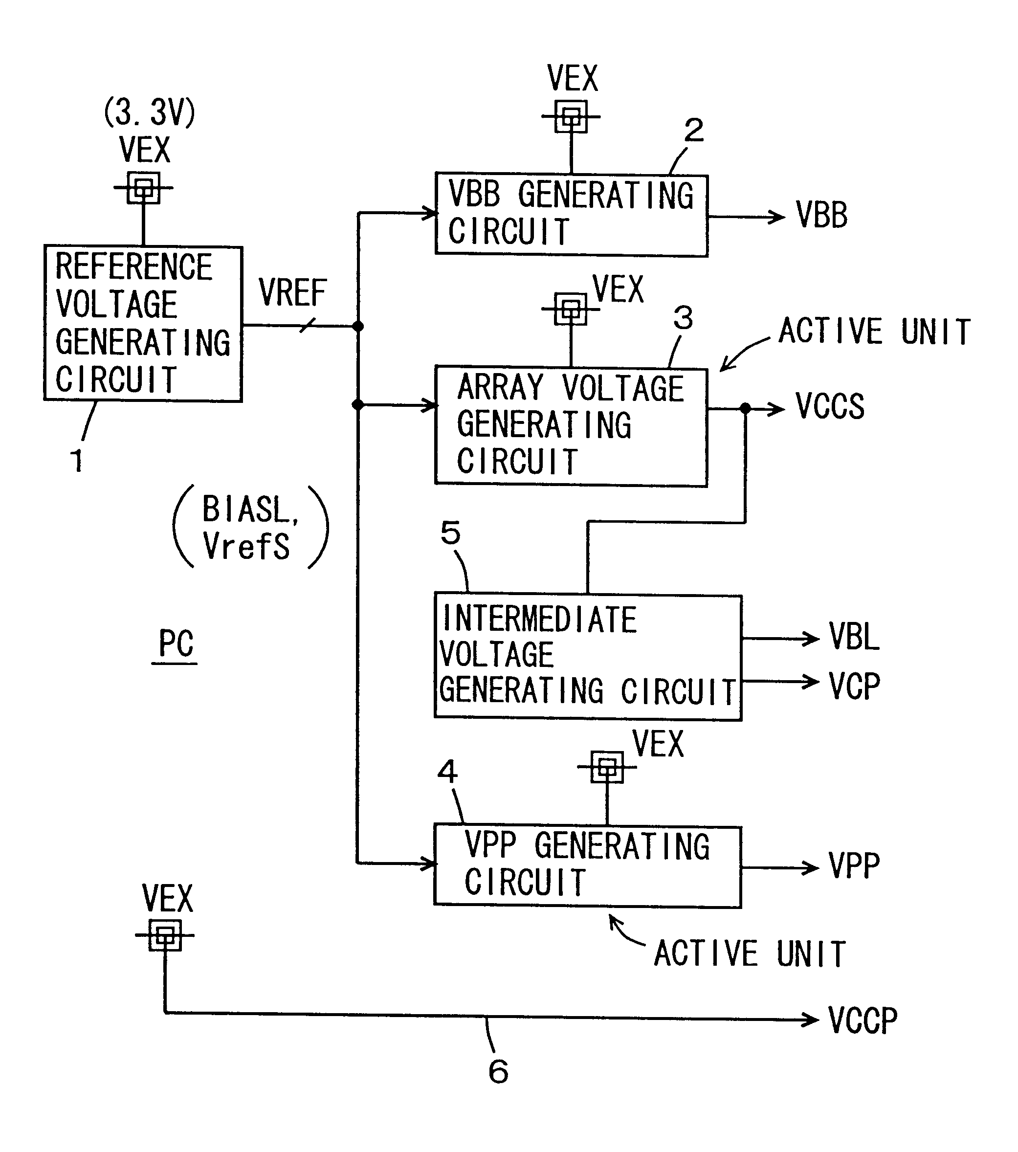
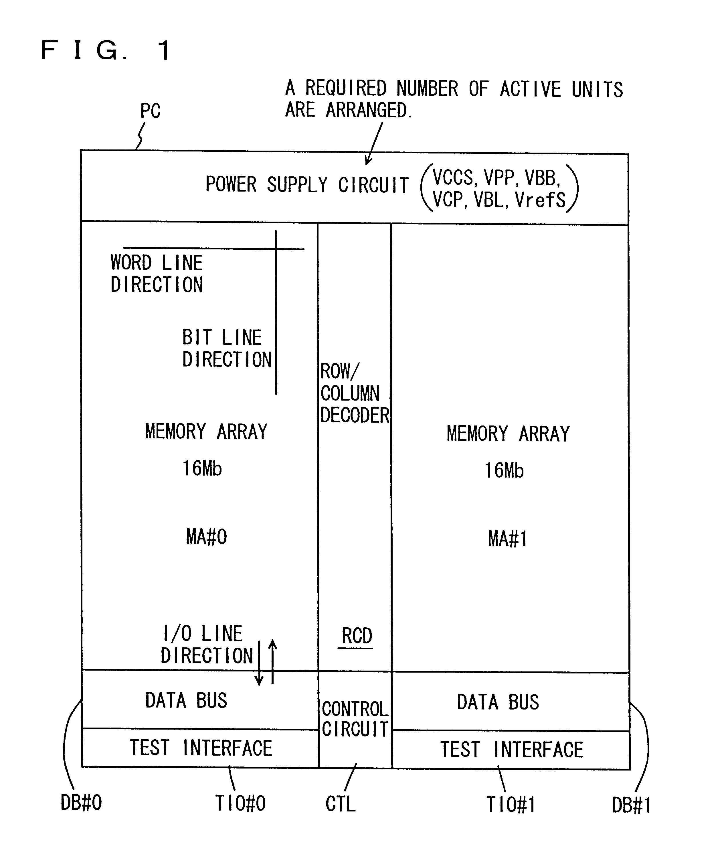
In the above description, the DRAM macro is assembled together with a logic in a mixed fashion. However, the invention can be applied also to the structure, in which DRAM (Dynamic Random Access Memory) is solely used.

The invention can be applied to various kinds of memories, provided that the memory includes a power supply circuit generating internal down-converted and / or boosted voltage.

According to the invention, as described above, the circuit supplying a large current is configured into an active unit in the form of cell, and the power supply line and the signal line required for this active unit are arranged in advance. Therefore, by changing only the arrangement of the active units or changing the number of employed active units, power supply circuits having various capabilities can be easily implemented. Even when the floor plan is changed in accordance with the storage capacity of a memory, no change is required for the power supply control circuits having small noise resist...


PUM


Abstract

An active down converting supplying a large current consumed when a memory array is active, and a Vpp pump for generating a boosted voltage are configured into active units as cells. A required number of active units are provided depending on the array structure and the operation conditions. A power supply circuit can be redesigned and/or rearranged within a short period for adaptation to change in internal structure for the memory array.

Description

1. Field of the InventionThe present invention relates to a semiconductor integrated circuit device, and particularly to a layout of an internal voltage generating circuit for generating an internal voltage utilized in the semiconductor integrated circuit device. More particularly, the invention relates to the structure of the internal voltage generating circuit suitable to a power supply for a Dynamic Random Access Memory (DRAM) included in a logic-merged memory, in which a semiconductor memory such as a DRAM and a logic are integrated on a single chip.2. Description of the Background ArtFIG. 47 schematically shows a chip layout of a conventional semiconductor integrated circuit device. In FIG. 47, a semiconductor integrated circuit device 900 includes pads 902 arranged on a periphery of a chip, a DRAM macro 903, and first, second and third merged circuits 905, 907 and 909 arranged in a region surrounded by pads 902. Each of these first to third merged circuits 905, 907 and 909 is ...

Claims


Application Information

Patent Timeline
IPC IPC(8): G11C5/14G11C11/407G11C11/401H01L21/822H01L27/04
CPCG11C5/14G11C5/147G11C5/145
Inventor MORISHITA, FUKASHI
Owner RENESAS ELECTRONICS CORP
Why Eureka
Try Eureka