Charge pump circuit

a charge pump and circuit technology, applied in the direction of automatic control, process and machine control, instruments, etc., can solve the problems of charge injection, coupling effect, integration errors,

Inactive Publication Date: 2003-03-18
SAMSUNG ELECTRONICS CO LTD
View PDF11 Cites 85 Cited by
  • Summary
  • Abstract
  • Description
  • Claims
  • Application Information

AI Technical Summary

Problems solved by technology

However, the conventional charge pump circuit shown in FIG. 1 has a problem in that a coupling effect occurs due to overlap gate-to-drain capacitance Cca of the first switching device 104 and overlap gate-to-drain capacitance Ccb of the second switching device 108.
Furthermore, the conventional charge pump circuit shown in FIG. 1 has a problem in that charge injection occurs due to parasitic capacitance Cpa existing at a junction N1 between the pull-up current source 102 and the first switching device 104, and parasitic capacitance Cpb existing at a junction N2 between the pull-down current source 106 and the second switching device 108.
The presence of coupling and charge injection may result in integration errors.
Thus, to achieve these characteristics, the charge pump circuit has disadvantages in that the layout area of the unity gain buffer 122 is increased and a large amount of power is consumed.

Method used


Image

  • Charge pump circuit
  • Charge pump circuit
  • Charge pump circuit

Examples


first embodiment

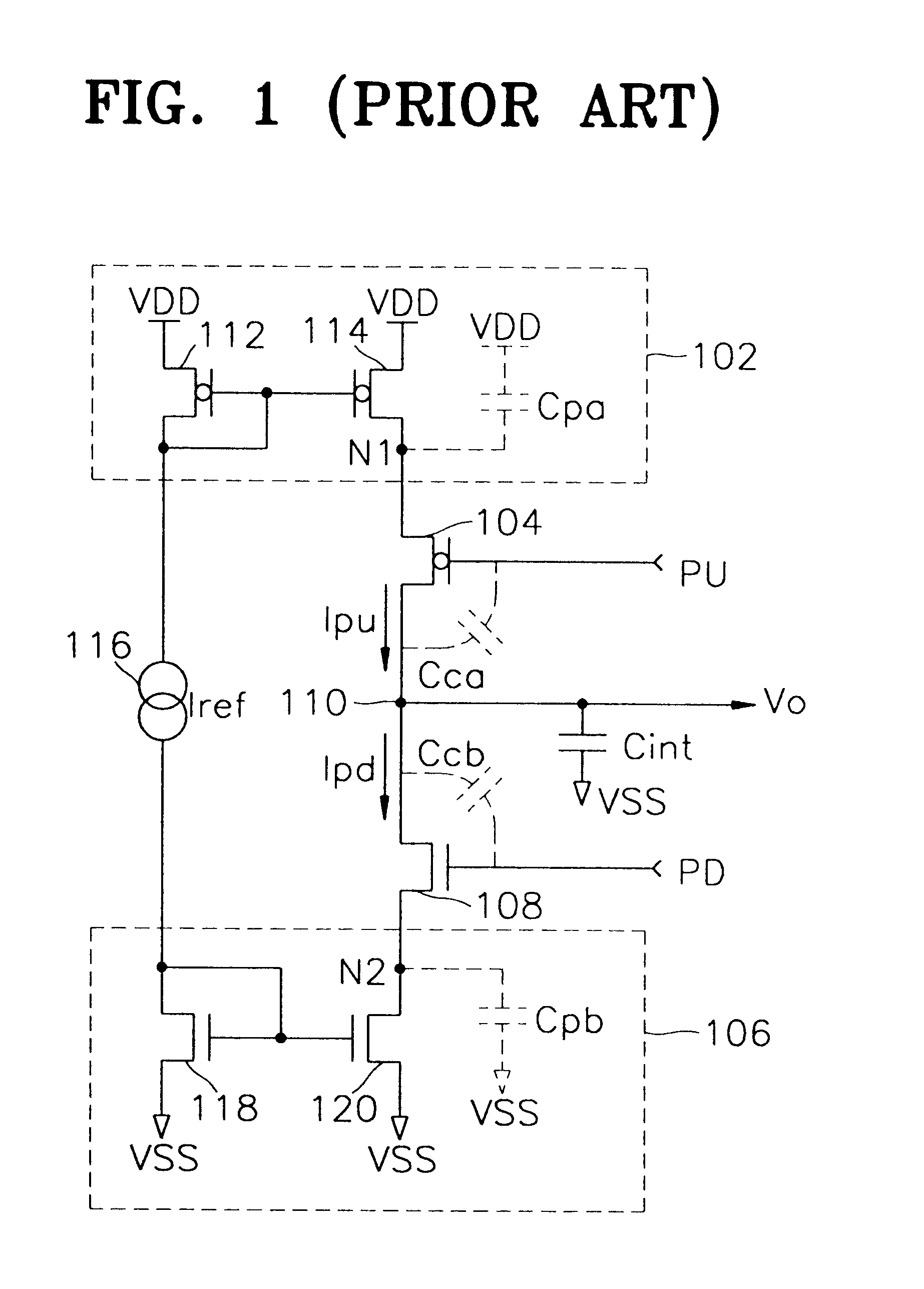
Referring to FIG. 3, a charge pump circuit according to the present invention includes a pull-up current source 302, a first switching device 304, a pull-down current source 306, a second switching device 308, an integration capacitor Cint, and a reference current source 316.

The pull-up current source 302 sources pump-up current Ipu to an output node 310 depending on predetermined reference current Iref that flows from the reference current source 316. The pull-up current source 302 includes a current mirror comprised of PMOS transistors 313 and 314, and a PMOS transistor 312 which is connected between the PMOS transistor 313 and a power voltage node VDD and to whose gate a ground voltage VSS is applied. The first switching device 304 comprised of, in one embodiment, a PMOS transistor, is connected between a power voltage VDD and the pull-up current source 302, and is switched in response to a pump-up control signal PU. The size of the PMOS transistor 312 is preferably the same as t...

second embodiment

The other end of the first dummy capacitor 501 is connected to an inverted signal PU of the pump-up control signal, and the other end of the second dummy capacitor 502 is connected to an inverted signal PD of the pump-down control signal. Thus, the charge pump circuit according to the invention does not suffer from a coupling effect because overlap capacitances Cca and Ccb are offset by the first and second dummy capacitors 501 and 502. As shown in the waveform diagram of FIG. 6, the waveform of an output signal V.sub.O is linear without overshoot.

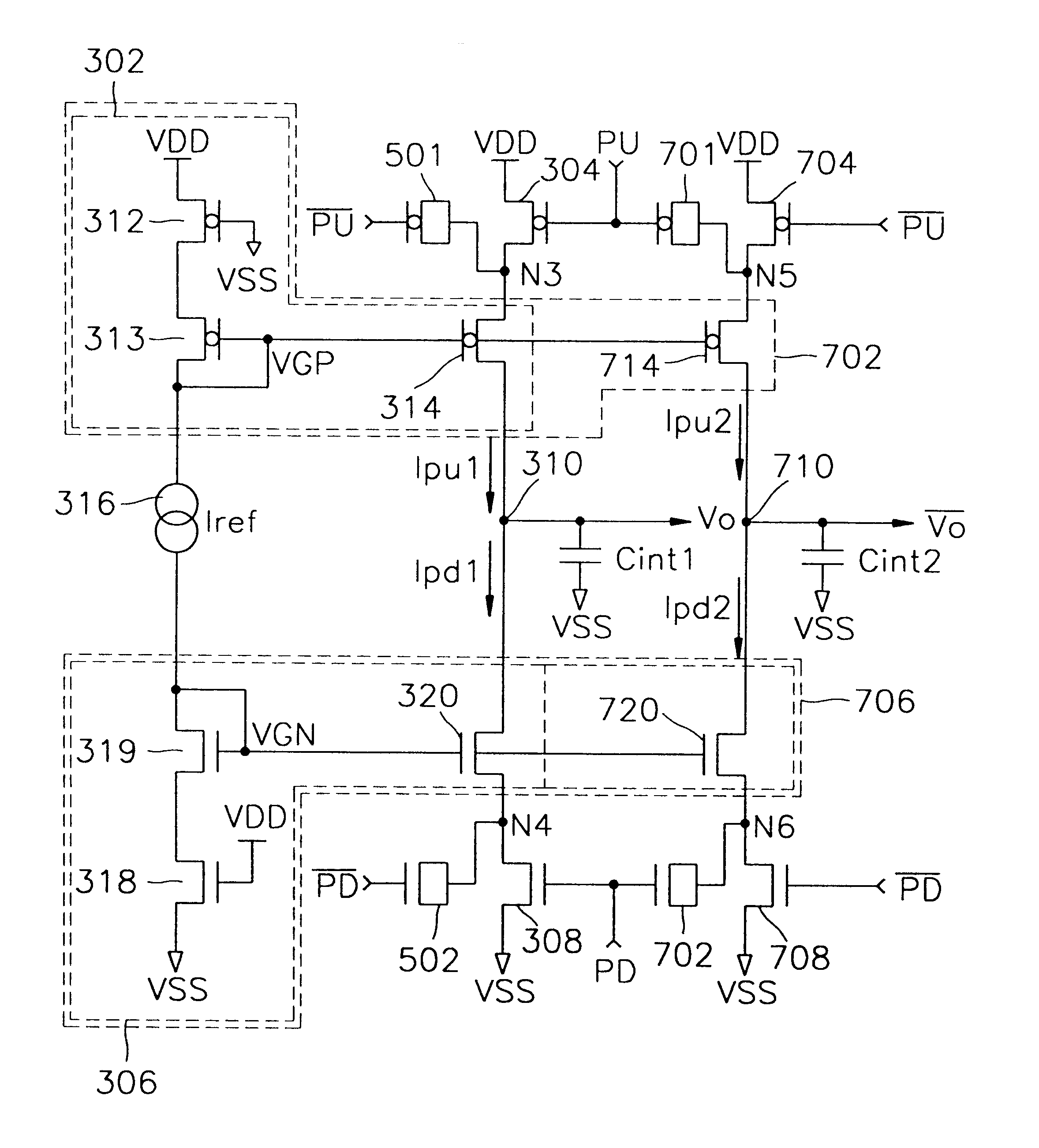
FIG. 7 is a circuit diagram of a charge pump circuit according to a third embodiment of the invention. Referring to FIG. 7, the charge pump circuit according to the third embodiment of the invention includes a first pull-up current source 302, a first switching device 304, a first pull-down current source 306, a second switching device 308, a first integration capacitor Cint1, a reference current source 316, a first dummy capacitor 501, an...

third embodiment

The second integration capacitor Cint2 is connected between the inverted output node 710 and a ground voltage node VSS, and integrates current flowing through the inverted output node 710 to change the current into the inverted voltage signal Vo. The third dummy capacitor 701 is connected between a junction N5 between the third switching device 704 and the second pull-up current source 702, and a pump-up control signal PU. The fourth dummy capacitor 702 is connected between a junction N6 between the fourth switching device 708 and the second pull-down current source 706, and a pump-down control signal PD. Thus, the differential type charge pump circuit according to the invention does not suffer from a coupling effect because overlap capacitances are offset by the first through fourth dummy capacitors 501, 502, 701, and 702.

As has been described in the foregoing, in a charge pump circuit according to the invention, a switching device controlled by a pump-up control signal PU or an in...


PUM


Abstract

A charge pump circuit capable of preventing coupling and charge injection without increasing a layout area and power consumption is provided. The charge pump circuit includes a pull-up current source, a pull-down current source, a first switching device, and a second switching device. The pull-up current source sources pump-up current to the output node. The pull-down current source includes a current mirror and sinks pump-down current from the output node. In particular, the first switching device is connected between a supply voltage node and the pull-up current source and is switched in response to a pump-up control signal. The second switching device is connected between the second current source and a ground voltage node and is switched in response to a pump-down control signal. The current pump circuit may further include a first dummy capacitor one end of which is connected to a junction between the first switching device and the first current source and a second dummy capacitor one end of which is connected to a junction between the second switching device and the second current source.

Description

1. Field of the InventionThe present invention relates to a semiconductor integrated circuit, and more particularly, to a charge pump circuit adopted in a delay locked loop (DLL) or a duty cycle correction circuit.2. Description of the Related ArtCharge pump circuits are used as integrators when a node of a circuit needs to be charged to a predetermined voltage level. When a charge pump circuit is used in a DLL, the charge pump circuit serves to receive a pump-up control signal or a pump-down control signal and integrate them. When a charge pump circuit is used in a duty cycle correction circuit, the charge pump circuit receives a clock signal to integrate a logic "high" interval of the clock signal with a negative (or positive) slope and integrate a logic "low" interval of the clock signal with a positive (or negative) slope. If a duty cycle of the clock signal is on the order of 50%, a constant voltage is output, if a duty cycle is below 50%, an increasing (or decreasing) voltage ...

Claims


Application Information

Patent Timeline
Patent Type & Authority Patents(United States)
IPC IPC(8): H03L7/089H03L7/08H03L7/093
CPCH03L7/0896H03L7/0895G05F3/24
Inventor KIM, KYU-HYOUN
Owner SAMSUNG ELECTRONICS CO LTD
Why Eureka
Try Eureka