Organic light emitting devices

Inactive Publication Date: 2003-04-22
INNOLUX CORP
View PDF4 Cites 15 Cited by
  • Summary
  • Abstract
  • Description
  • Claims
  • Application Information

AI Technical Summary

Problems solved by technology

Such potential drops would otherwise im

Method used


Image

  • Organic light emitting devices
  • Organic light emitting devices
  • Organic light emitting devices

Examples


Embodiment Construction

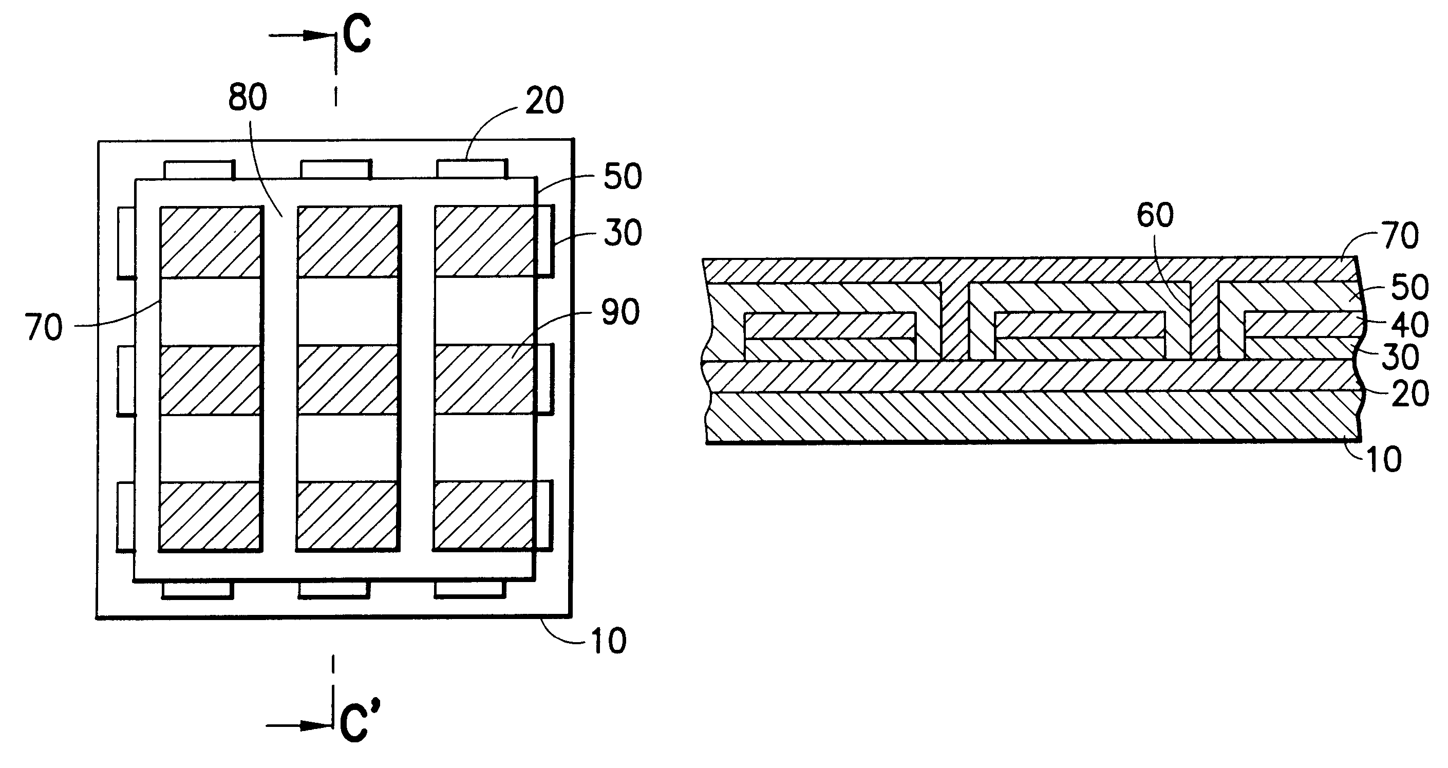
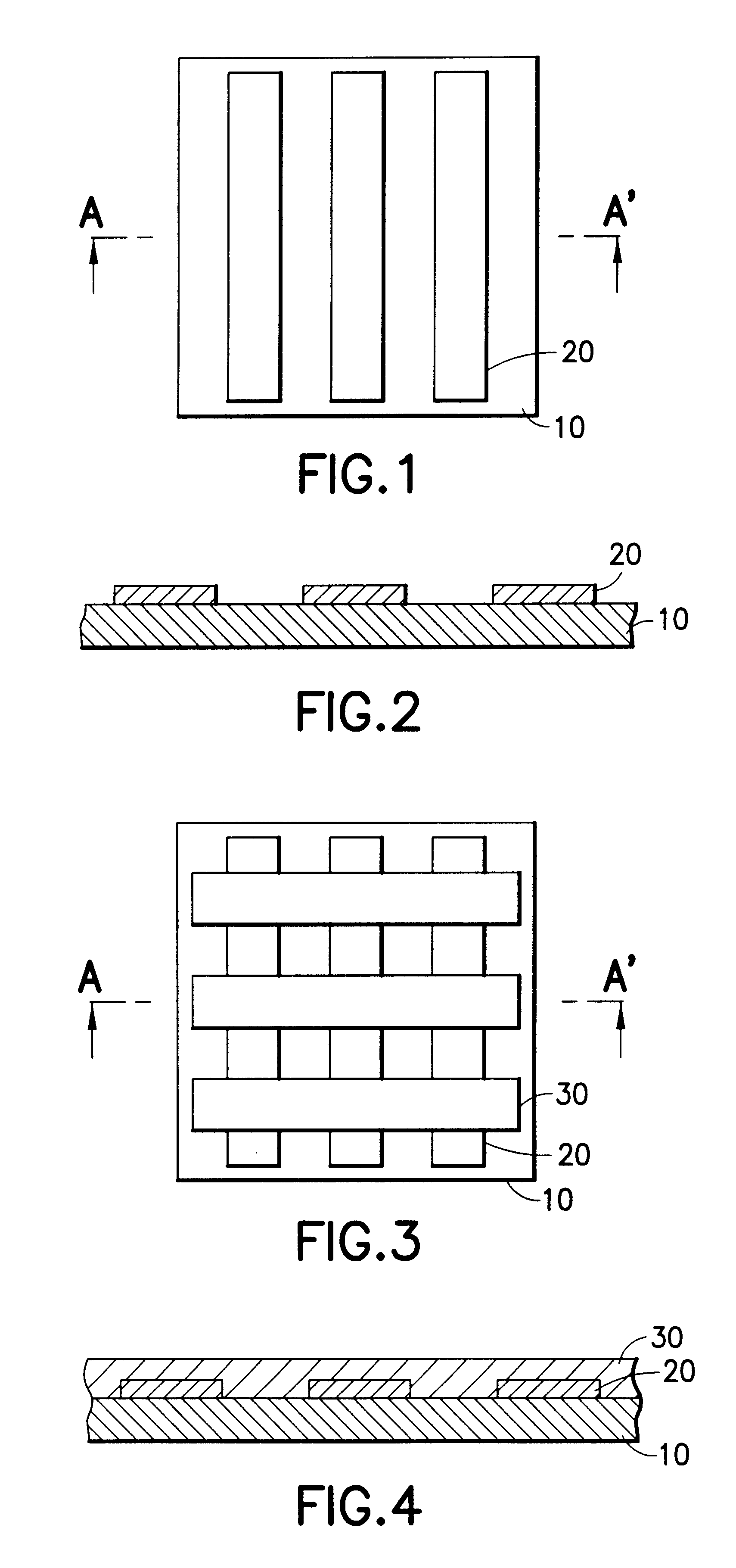
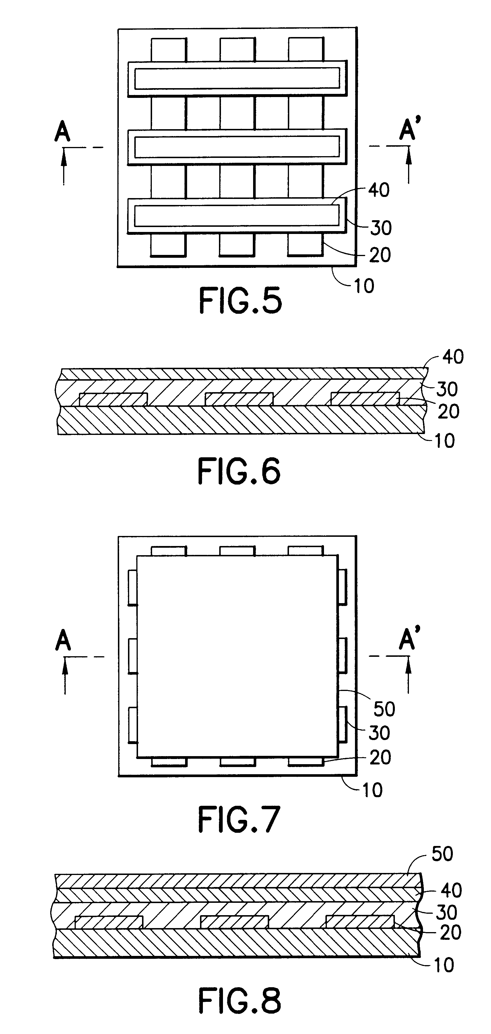
What follows now is a description of a passive matrix OLED embodying the present invention and methods for fabricating such an OLED.

Referring first to FIGS. 1 and 2 in combination, in a preferred embodiment of the present invention, first electrode layer of electrically conducting material 20 is deposited on a substrate 10. The substrate 10 may be formed from a light transmissive material such as glass or plastics or from an opaque material such as a Silicon wafer. The first electrode layer 20 may be formed from a range of different materials, including but not limited to Indium Tin Oxide, Indium Zinc Oxide, Aluminum Zinc Oxide, Aluminum, Nickel, Copper, Platinum, and Iridium, or combinations of the aforementioned materials with organic and / or inorganic charge injection layers. The first electrode layer 20 comprises an array of parallel strips. In particularly preferred embodiments of the present invention, the strips of the first electrode layer 20 can be formed by evaporation and ...


PUM


Abstract

An organic light emitting device has a layer structure having: a first electrode layer; a second electrode layer parallel to the first electrode layer; and, an electrically conductive and light transmissive layer parallel to the second electrode layer. An electrically insulating layer is disposed between the first and second electrode layers. A layer of organic material is disposed between the second electrode layer and the conductive layer. An aperture in the organic layer provides an electrical connection path between the conductive layer and one of the first and second electrode layers.

Description

Field of the InventionThe present invention relates to organic light emitting devices for display applications and to methods for fabricating such devices.Background ArtOrganic light-emitting devices (OLEDs) are typically manufactured as a sequence of layers deposited on top of each other to form a layer structure. The layer structure typically comprises a first electrode on a supporting substrate and several organic layers disposed between the first electrode and a second electrode. Light output is generated by charge injection into the organic material via the electrodes. The organic material emits photons on excitation by the injected charge. At least one of the electrodes is typically formed from a light transmissive material such as Indium Tin Oxide (ITO) or a thin metal to permit passage of light out of the device.In accordance with the present invention, there is now provided an organic light emitting device having a layer structure comprising: a first electrode layer; a seco...

Claims


Application Information

Patent Timeline
IPC IPC(8): H01L27/28H01L27/32
CPCH01L27/3281H01L51/5212Y10S257/918H10K59/17H10K50/814
Inventor BECK, ARMINBEIERLEIN, TILMAN A.MUELLER, PETERRIEL, HEIKERIESS, WALTER HEINRICH
Owner INNOLUX CORP
Why Eureka
Try Eureka