High bit density, high speed, via and metal programmable read only memory core cell architecture

a core cell and memory technology, applied in the field of electronic circuits, can solve the problems of increasing the resistance of an access transistor, reducing the speed, and increasing the complexity of integrated circuits, and achieve the effects of high bit density, fast turn around time, and high speed

Inactive Publication Date: 2003-04-29
STMICROELECTRONICS LTD
View PDF4 Cites 9 Cited by
  • Summary
  • Abstract
  • Description
  • Claims
  • Application Information

AI Technical Summary

Benefits of technology

These and other objects, features, and advantages in accordance with the present invention are provided by a high bit density, high speed, via and metal BE type programmable ROM core cell architecture for storing large amounts of non-volatile data and having a relatively fast turn around time. The ROM core cell may include memory cells organized on a row and column basis where each of the memory cells includes three transistors and two bit lines. The arrangement between the three transistors and the two bit lines may be such that each of the memory cells is capable of storing four bits of data.
More particularly, the transistors may be MOS transistors. Any two of the three transistors may be capable of storing one bit of data in their respective drains and another bit of data in thei

Problems solved by technology

The complexity of integrated circuits is continually increasing.
Though a conventional BE programmable ROM has the advantage of fast time to market, it may suffer from the following disadvantages: the area of a BE programmable ROM memory cell is 30%-40% more than that of an FE programmable ROM memory

Method used


Image

  • High bit density, high speed, via and metal programmable read only memory core cell architecture
  • High bit density, high speed, via and metal programmable read only memory core cell architecture
  • High bit density, high speed, via and metal programmable read only memory core cell architecture

Examples


Embodiment Construction

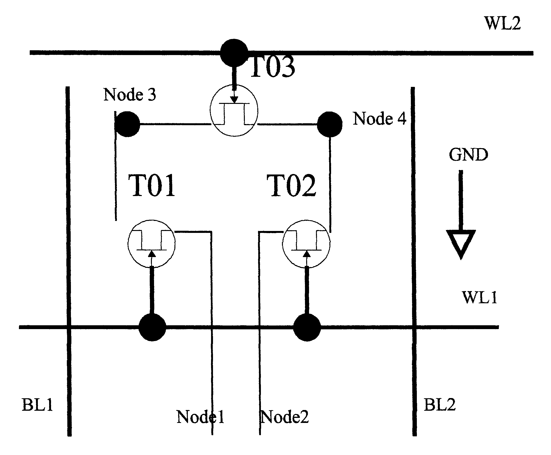
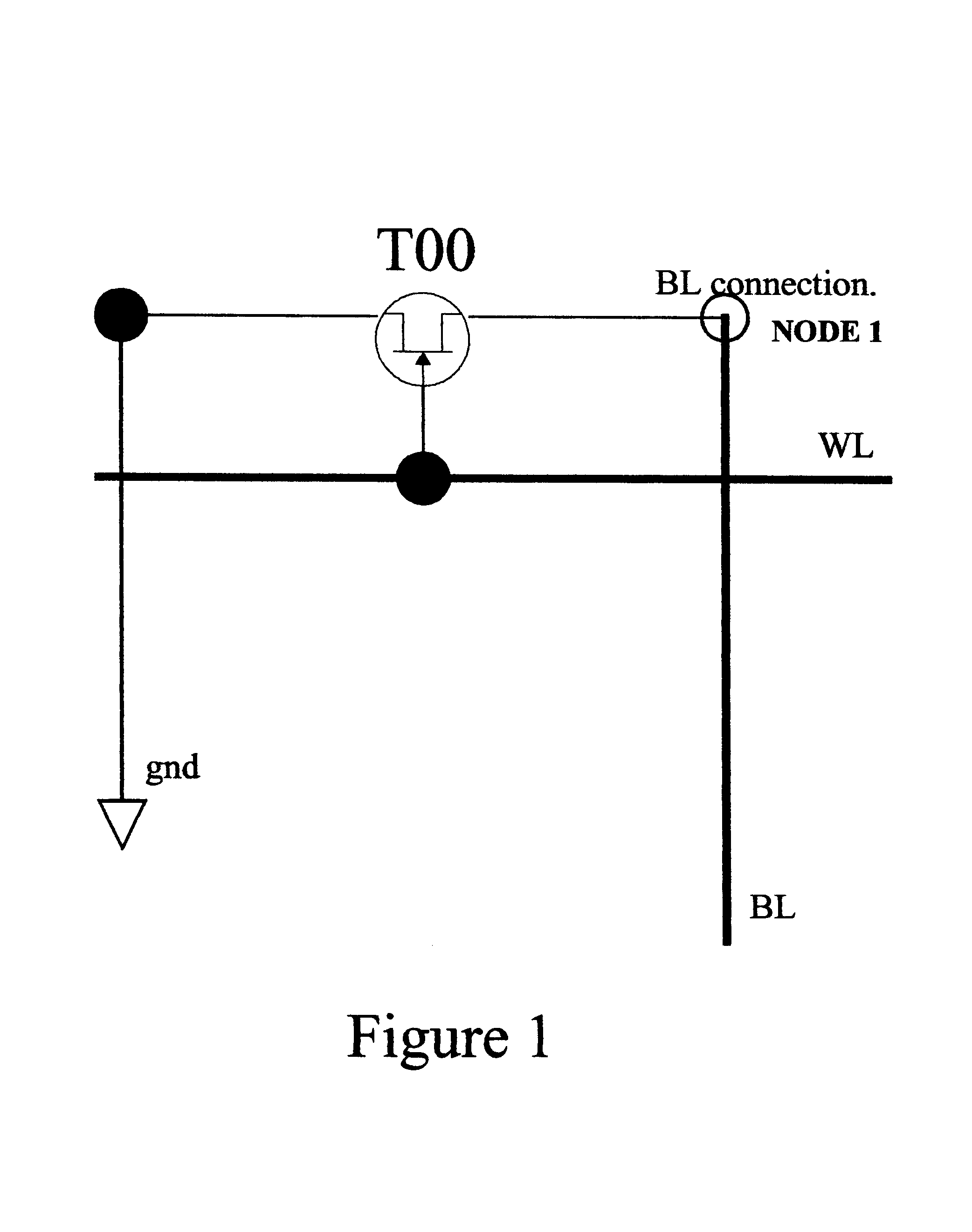
Referring now to FIG. 3, a ROM core architecture having a memory cell including three MOS transistors T01, T02, T03 in accordance with the present invention is shown. In this memory cell, four bits of information can be stored. That is, four bits of information may be stored on the three MOS transistors T01, T02, T03 by programming the drain and source of the transistors.

Programming the ROM core architecture according to the present invention will be more clearly understood with reference to FIG. 3. Bit lines BL1, BL2 and transistors T01, T02, T03 together form one memory cell. For programming transistor T01, bit lines BL1, BL2 and GND are needed. Node 1 of the transistor T01 has bit line BL1 as its bit line. Bit line BL1 will be accessed to determine the data at node 1. Initially, all bit lines BL1, BL2, etc. are held to ground GND. When a bit line is selected (e.g., BL1), it is pre-charged to a voltage VDD. All other bit lines are held to GND.

In the row controlled by word line WL1...


PUM


Abstract

A high bit density, high speed, via and metal BE type programmable ROM core cell architecture for storing large amounts of non-volatile data and having a relatively fast turn around time is provided. The ROM core cell may include memory cells organized in rows and columns where each of the memory cells includes three transistors and two bit lines. The arrangement between the three transistors and two bit lines may be such that each of the memory cells is capable of storing four bits of data.

Description

FIELD OF THE INVENTIONThe present invention relates to the field of electronic circuits, and, more particularly, to memory devices. More specifically, the invention relates to a high bit density, high speed, via and metal BE type programmable read only memory (ROM) core cell architecture for storing of large amounts of non-volatile data which provides a relatively fast turn around time.BACKGROUND OF THE INVENTIONThe complexity of integrated circuits is continually increasing. As a result, there is need for high bit density ROMs that can store large amounts of non-volatile data and that allow quick access thereto. In today's competitive market, the time to market an electronic device needs to be as short as possible. Thus, when ROMs are used in such electronic devices, the ROMs should provide for a short turn around time. The turn around time primarily depends upon the fabrication stage at which programming of non-volatile data is done. If the programming is done at a later stage of ...

Claims


Application Information

Patent Timeline
IPC IPC(8): G06F13/28G06F12/00G06F12/16G06F13/00G06F12/14G06F13/20G11C17/00
CPCG11C17/16G11C11/5692G06F2213/0038
Inventor GARG, ANURAG
Owner STMICROELECTRONICS LTD
Why Eureka
Try Eureka