Method of reducing disturbs in non-volatile memory

a non-volatile memory and disturb technology, applied in the field of non-volatile memory, can solve problems such as loss of electric charge in floating gate gain or loss, defect and failure of eeproms and flash eeproms,

Inactive Publication Date: 2003-05-27
SANDISK TECH LLC
View PDF11 Cites 155 Cited by
  • Summary
  • Abstract
  • Description
  • Claims
  • Application Information

AI Technical Summary

Problems solved by technology

As with most devices, EEPROMs and Flash EEPROMs are susceptible to defects and failures.
One way errors can occur is by the shifting of the threshold level of the memory states.
Other cells within the same column are not addressed since their word lines are non-selected and placed at zero potential; nevertheless, they may be affected by the program operation of the addressed cell because of the high voltage on the common bit line and the other bit lines as well.
This may induce electric charge leakage in these non-addressed cells, resulting in either a gain or loss of electric charge in their floating gate depending on the electrical mechanism.
However, the number or severity of the errors can become sufficient to overwhelm these methods and result in a degradation of the data stored in the memory.
It has been found that a source of disturbs is the displacement current generated in non-selected word lines of an array that results when the voltage levels on array's bit lines are changed.
Because of the non-perfect conductivity of the word lines, this induced current results in a voltage developed on the control gates of memory cells along the non-selected word lines and, consequently, may result in disturbs.

Method used


Image

  • Method of reducing disturbs in non-volatile memory
  • Method of reducing disturbs in non-volatile memory
  • Method of reducing disturbs in non-volatile memory

Examples


Embodiment Construction

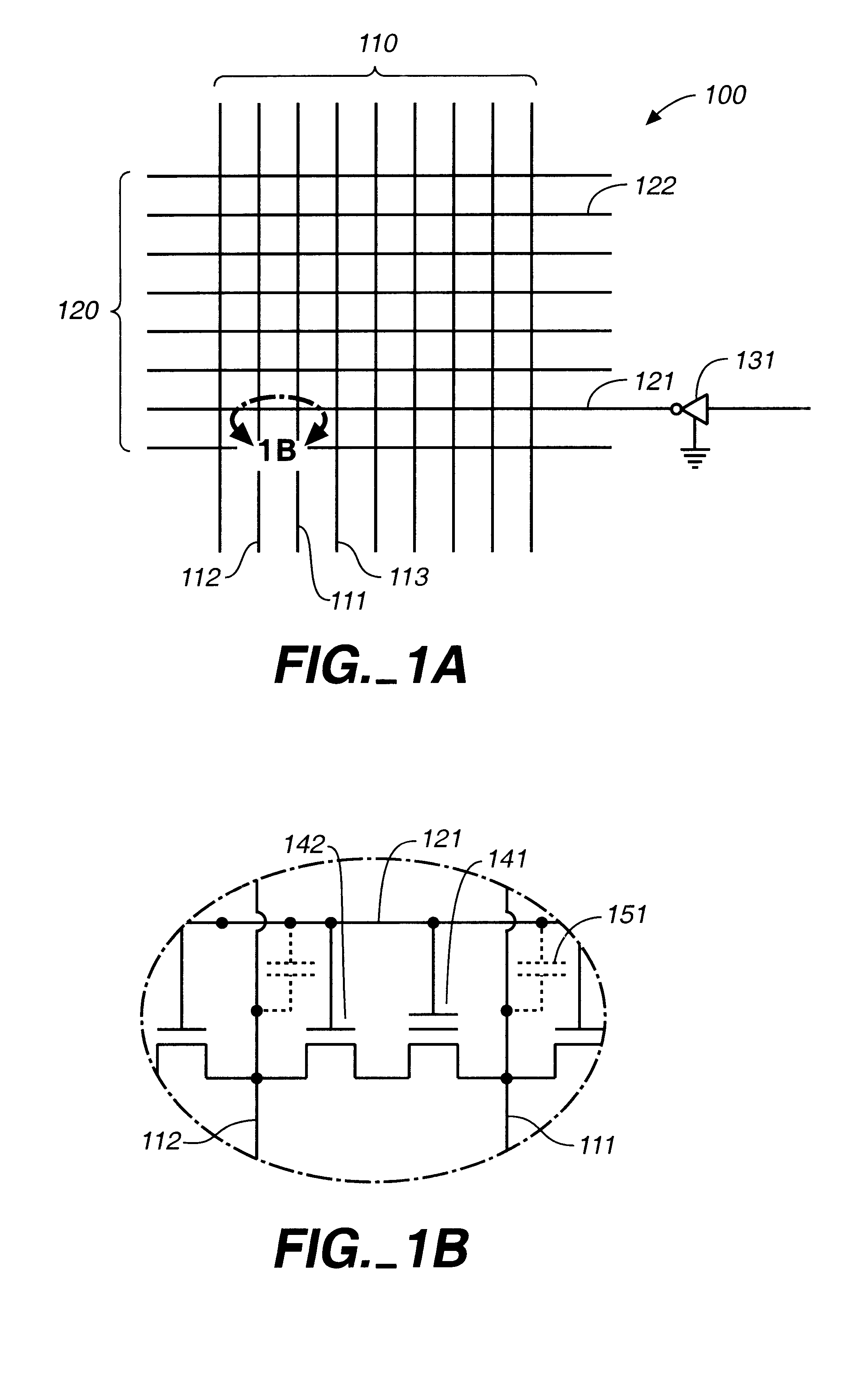
It has been discovered that disturbs are introduced into a memory array due to displacement currents in non-selected word lines resulting from the rate of change in the voltage levels on the bit lines. Returning to the simplified situation of FIG. 1, consider the case where the cell connected between bit lines 111 and 112, with its control gate connected to word line 122, is to be programmed. The bit line 111 will be raised to a voltage V.sub.b1 of, say, 5 volts relative to bit line 112. The voltage change on bit line 111 will occur over a finite rise time and is characterized by the rate dV.sub.bl / dt. Other cells along the selected word line 122 which are being programmed will similarly have their bit lines raised. The word line 122 is then pulsed with a programming voltage, a verification usually being performed between programming pulses. For the non-selected word lines, such as 121, where the cells are not being programmed, a word line driver such as 131 sets these word lines t...


PUM


Abstract

In a non-volatile memory, the displacement current generated in non-selected word lines that results when the voltage levels on an array's bit lines are changed can result in disturbs. Techniques for reducing these currents are presented. In a first aspect, the number of cells being simultaneously programmed on a word line is reduced. In a non-volatile memory where an array of memory cells is composed of a number of units, and the units are combined into planes that share common word lines, the simultaneous programming of units within the same plane is avoided. Multiple units may be programmed in parallel, but these are arranged to be in separate planes. This is done by selecting the number of units to be programmed in parallel and their order such that all the units programmed together are from distinct planes, by comparing the units to be programmed to see if any are from the same plane, or a combination of these. In a second, complementary aspect, the rate at which the voltage levels on the bit lines are changed is adjustable. By monitoring the frequency of disturbs, or based upon the device's application, the rate at which the bit line drivers change the bit line voltage is adjusted. This can be implemented by setting the rate externally, or by the controller based upon device performance and the amount of data error being generated.

Description

1. Field of the InventionThis invention relates generally to non-volatile memories, and, more specifically, to methods of reducing disturbs in electrically erasable and programmable read only memories (EEPROMs).2. Background InformationA non-volatile memory cell stores information by altering the control gate voltage required to enable source-drain current conduction. This is known as the cell's threshold voltage, V.sub.t. Programming is the operation used to change this conduction threshold in order to store information on the cell. The memory cells are conventionally arranged in an array, with rows defined by word lines, columns defined by bit lines, and the cells identified by the word lines and bit lines to which they are attached.A portion of such an array of memory cells is shown schematically in FIG. 1. In this figure, the word lines 120 and bit lines 110 form a grid. The detail shows an example of how a cell may be place within this array. In this particular example, the cel...

Claims


Application Information

Patent Timeline
Patent Type & Authority Patents(United States)
IPC IPC(8): G11C16/06G11C16/12
CPCG11C16/12
Inventor MANGAN, JOHN S.GUTERMAN, DANIEL C.SAMACHISA, GEORGEMURPHY, BRIANWANG, CHI-MING
Owner SANDISK TECH LLC
Why Eureka
Try Eureka