Electro optic modulator

a technology of optical modulator and optical fiber, applied in the direction of optics, optical light guides, instruments, etc., can solve the problems of difficult control of dopant profiles, loss of signal and local heating,

Inactive Publication Date: 2003-06-24
BOOKHAM TECH
View PDF10 Cites 35 Cited by
  • Summary
  • Abstract
  • Description
  • Claims
  • Application Information

AI Technical Summary

Benefits of technology

The present invention seeks to provide an electro optic device in which the dopant pr

Problems solved by technology

This is because dopant elements tend to act as absorption sites for the light beam, leading to signal losses and local heating.
A difficulty in manufacturing the structure shown in FIG. 1 is that the dopant profile is difficult to co

Method used


Image

  • Electro optic modulator
  • Electro optic modulator
  • Electro optic modulator

Examples


Embodiment Construction

It should be noted that for convenience of description, terms such as "lateral", "vertical", "side", "top" etc. used in the specification refer to directions relative to a device in the orientation shown in the accompanying drawings. The terms should not, however, be interpreted as restricting the scope of the claimed invention which may in practice be used in any orientation.

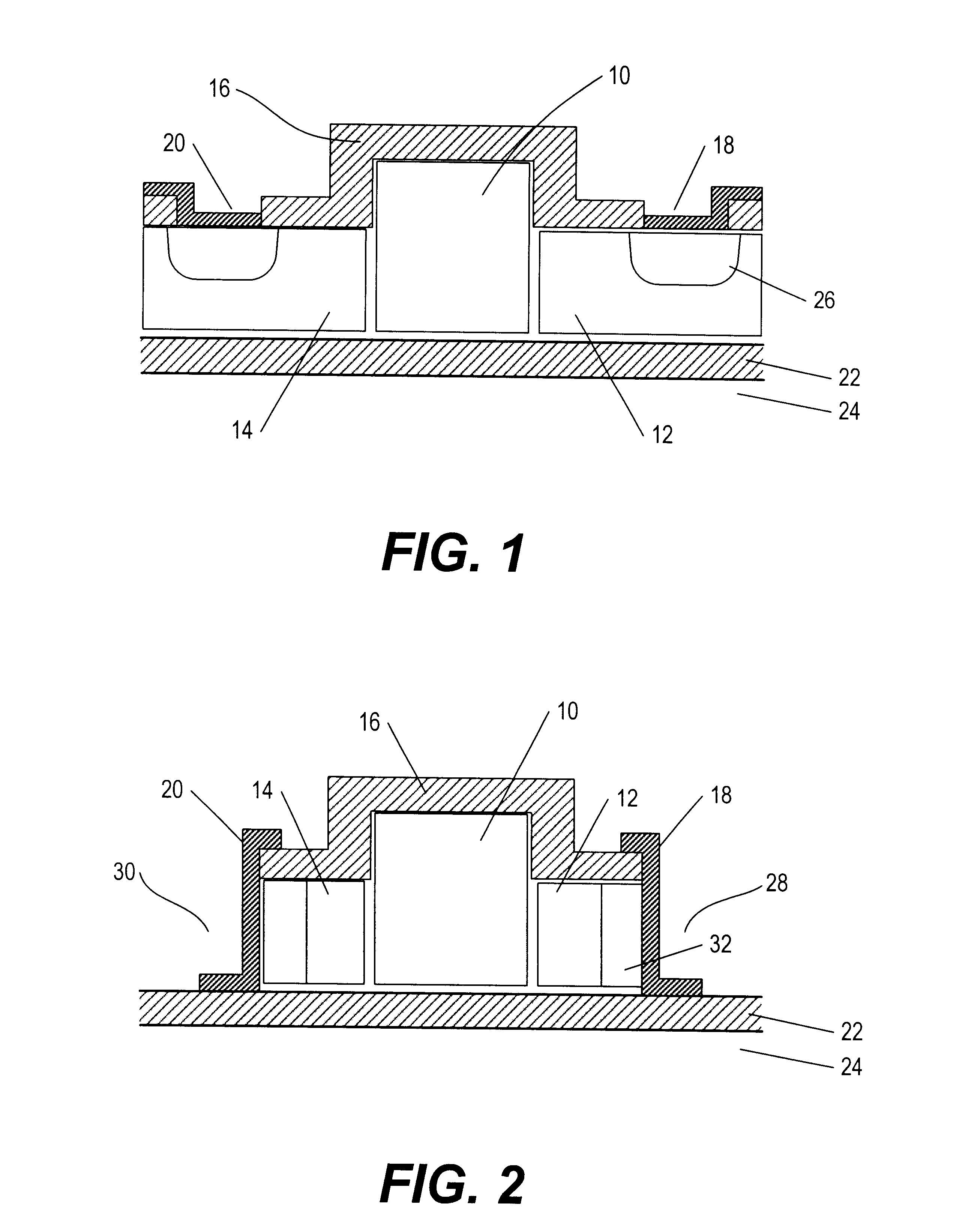
FIG. 1 has already been described in detail, and therefore no further description will be given here.

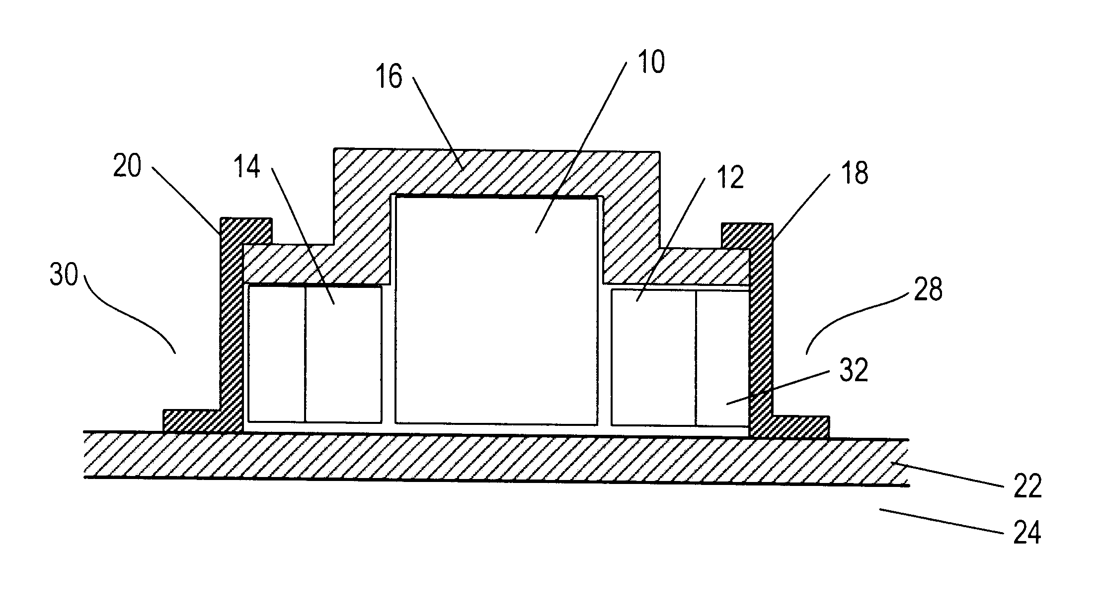
FIG. 2 shows a first embodiment of the present invention. As in FIG. 1, the device is a silicon-on-insulator device in which an oxide layer 22 lies between the active elements and an underlying silicon support 24. The ridge of the waveguide 10 is again flanked on either side by slab regions 12, 14, but these are now flanked by etched regions 28, 30 formed by an anistropic, directional dry etch. A protective oxide layer 16 covers the waveguide ridge 10 and the top surfaces of the slab regions 12, 14.
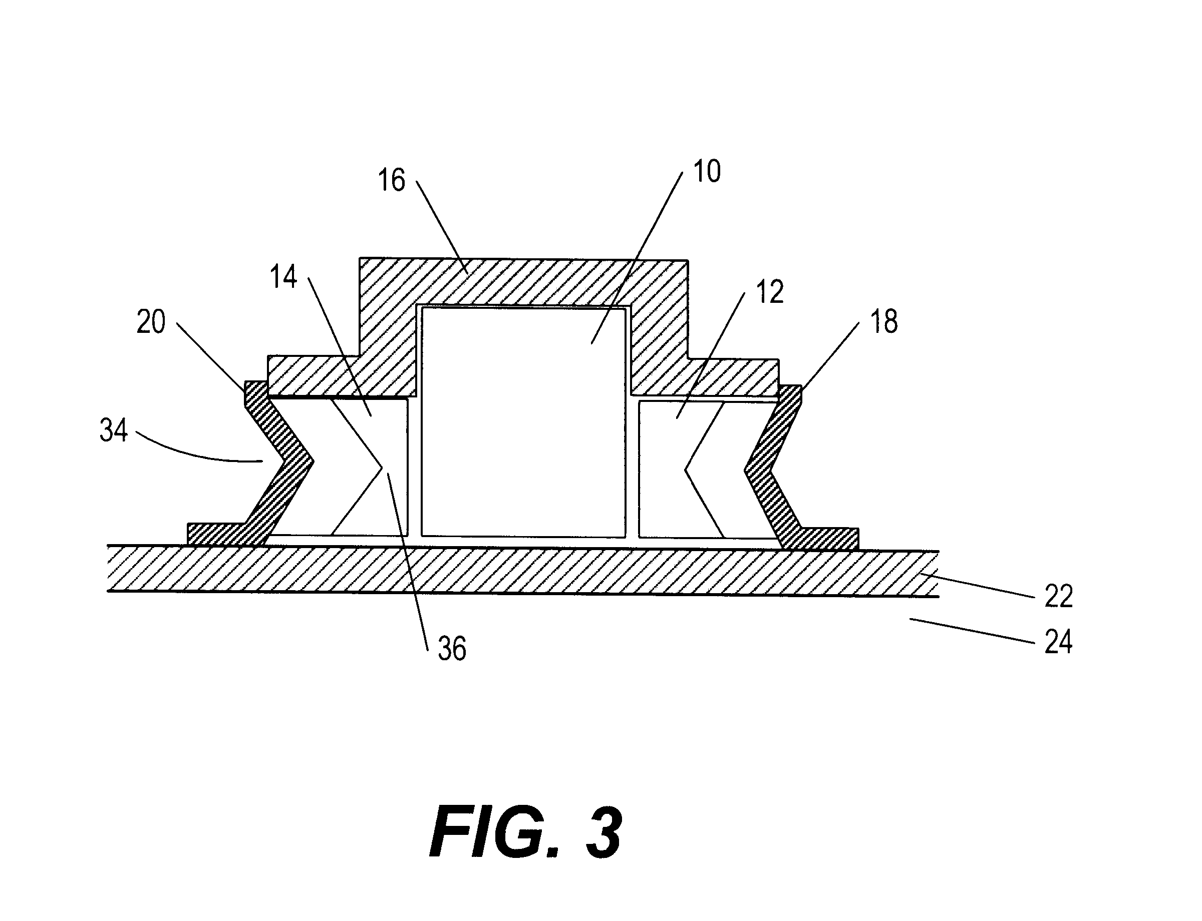
The slab regi...


PUM


Abstract

A doped slab region is described for use around a ridge waveguide, for controlling the refractive index of the waveguide material. Instead of simply diffusing dopant in from a surface of the slab region adjacent the waveguide, an area of the slab region is etched and dopant diffused in from a side face of the etched region. Thus, the dopant profile is established from a horizontal direction, allowing the profile to be controlled. A simple vertically uniform doping profile can thus be provided, leading to a vertically uniform current density, or an anisotropic wet etch can be applied after the initial etch to provide a profile which concentrates the current density at a selected height in the slab region.

Description

This invention relates to electro optic modulators.It is known to form p-i-n devices around ridge waveguide structures. A summary is shown in FIG. 1, where the ridge 10 is surrounded by a slab region 12, 14 on either side, together forming a single mode ridge waveguide. The device is protected with an oxide layer 16, in which openings 18, 20 are formed either side of the ridge 10. These regions are doped to form local p and n regions, thus creating a p-i-n diode across the waveguide. This can be used to manipulate the charge carrier concentration within the waveguide, thus controlling its refractive index. This can then be used to modulate a light beam passing through the waveguide. Alternatively, a n-i-n or p-i-p structure will be sufficiently conductive to provide a thermal phase modulator by controlling the refractive index through its temperature dependence. Such a structure is described in U.S. Pat. No. 5,757,986, which this application is a CIP application thereof and whose en...

Claims


Application Information

Patent Timeline
IPC IPC(8): G02F1/01G02F1/025
CPCG02F1/025
Inventor DAWNAY, EMMA JANE CLARISSAHARPIN, ARNOLD PETER ROSCOEDAY, IAN EDWARD
Owner BOOKHAM TECH
Why Eureka
Try Eureka