Semiconductor device with a voltage regulator

a technology of voltage regulator and semiconductor device, which is applied in semiconductor devices, digital storage, instruments, etc., can solve the problems of reducing the regulated voltage vreg, increasing the power consumption or dissipation of the integrated circuit concerned, and the penetration current of the booster circuit badly behaves to limit the booster performan

Inactive Publication Date: 2003-07-29
KIOXIA CORP
View PDF5 Cites 53 Cited by
  • Summary
  • Abstract
  • Description
  • Claims
  • Application Information

AI Technical Summary

Problems solved by technology

This results in a likewise decrease in the regulated voltage Vreg.
This penetration current would result in an increase in power consumption or dissipation of integrated circuits concerned.
Another problem faced with the prior art is that the flow of larger penetration current in booster circuitry badly behaves to limit the performance of the booster, i.e. voltage boost ability or "boostability," in view of the fact that most booster circuits for generation of the boosted voltage Vpp are less in current supplying abilities.
The limitation to boostability in turn leads to an increase in time as taken to create the boosted voltage Vpp and regulated voltage Vreg with potential trackability thereto.
In the worst case, any desired regulated voltages will no longer be obtainable in any way.

Method used


Image

  • Semiconductor device with a voltage regulator
  • Semiconductor device with a voltage regulator
  • Semiconductor device with a voltage regulator

Examples


Embodiment Construction

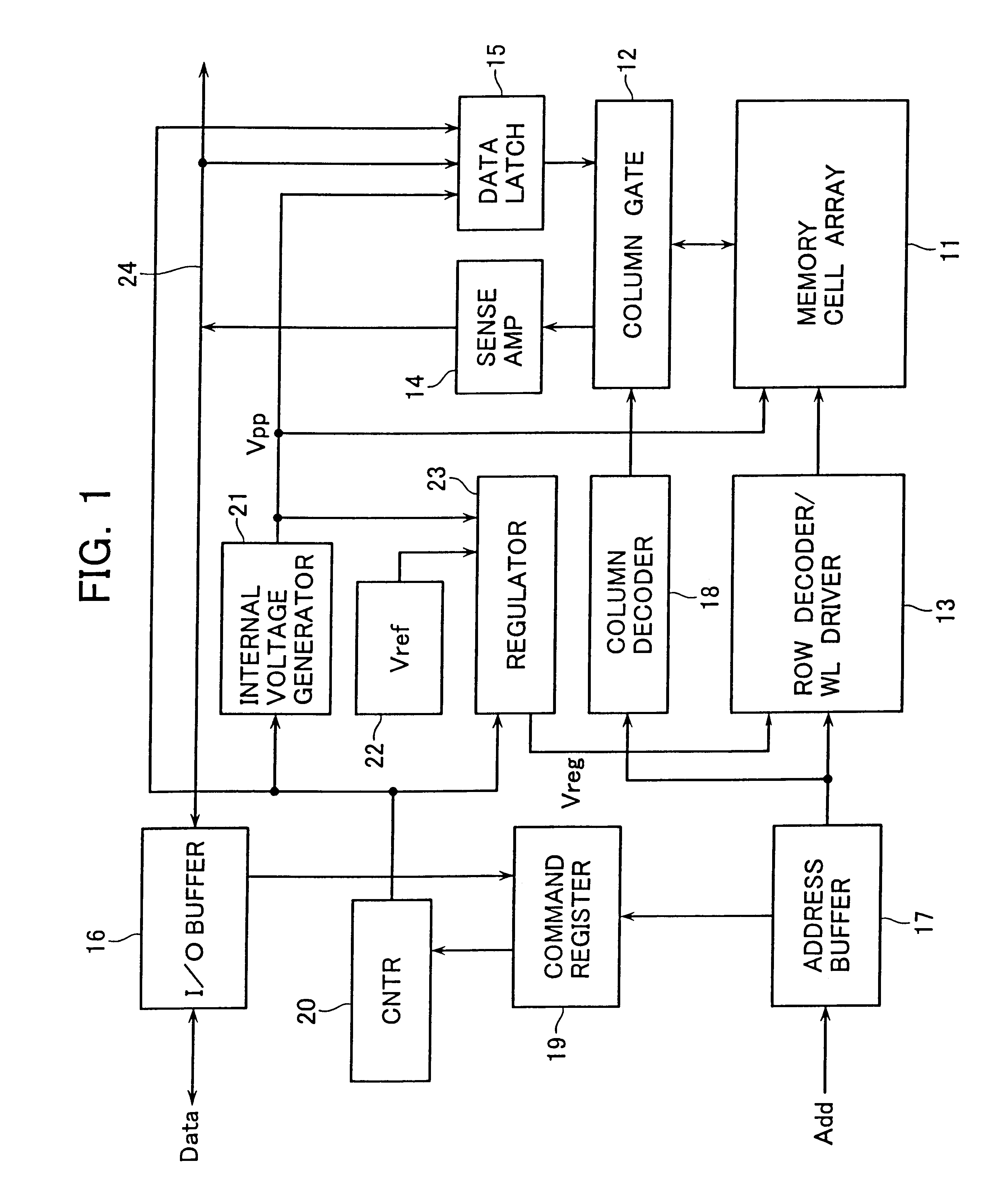
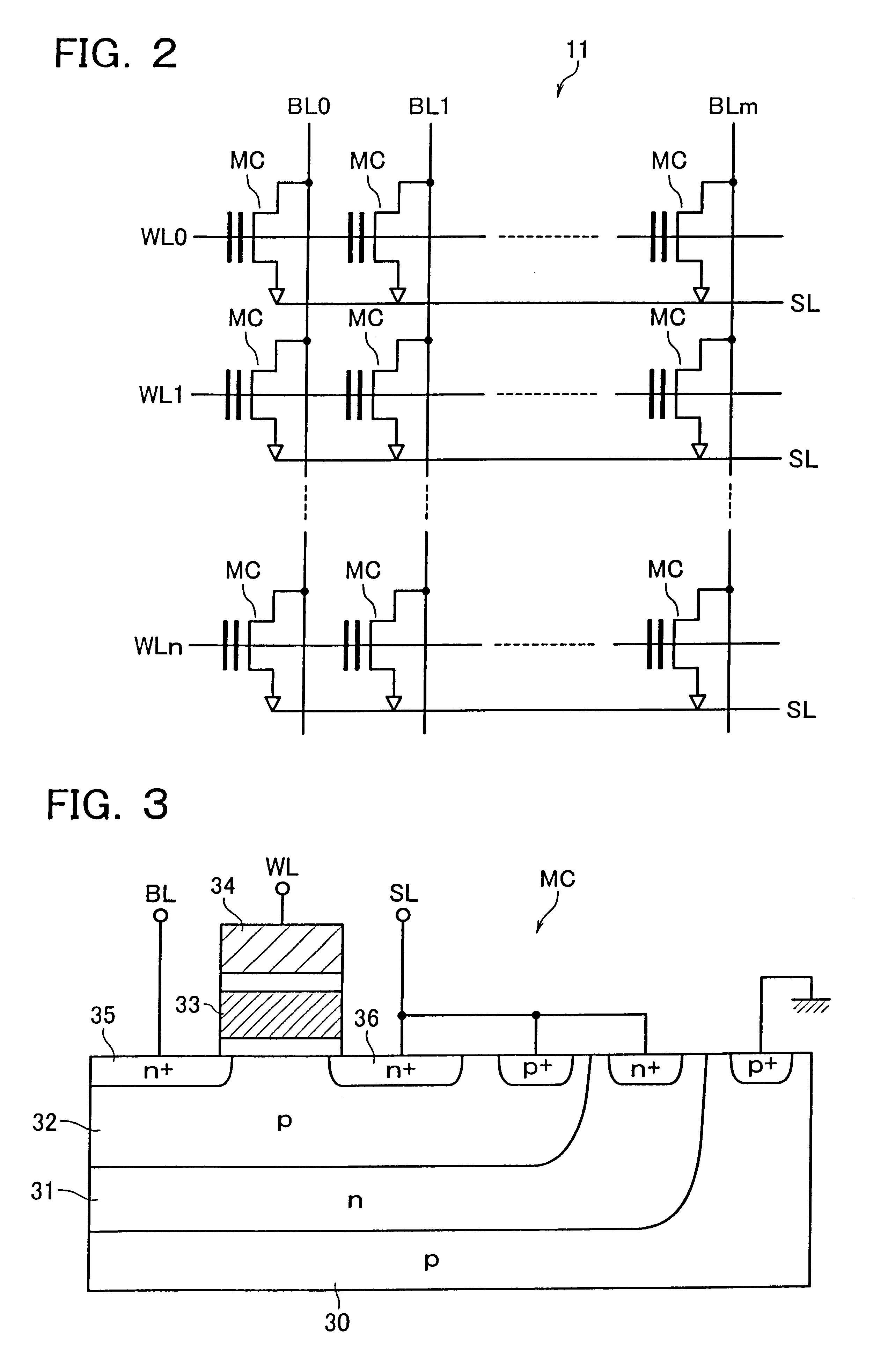
Referring now to FIG. 1, there is shown an overall configuration of a "Flash" EEPROM chip of the NOR type, which incorporates the principles of this invention. This Flash NOR-EEPROM includes an array 11 of rows and columns of memory cells. As shown in FIG. 2, this memory cell array 11 is constituted from a plurality of nonvolatile memory cells MC as organized into a matrix form. As shown in FIG. 3, each memory cell MC is formed of a metal oxide semiconductor field effect transistor (MOSFET) of the stacked gate structure type, with a floating gate 33 and a control gate 34 being stacked above a silicon substrate 30. Drains 35 of a column of memory cells MC are connected in common to a corresponding one of parallel bit lines BL whereas control gates 34 of a row of memory cells MC are commonly coupled to one of parallel word lines WL crossing over the bitlines BL. Their sources 36 are coupled to a common source line SL.

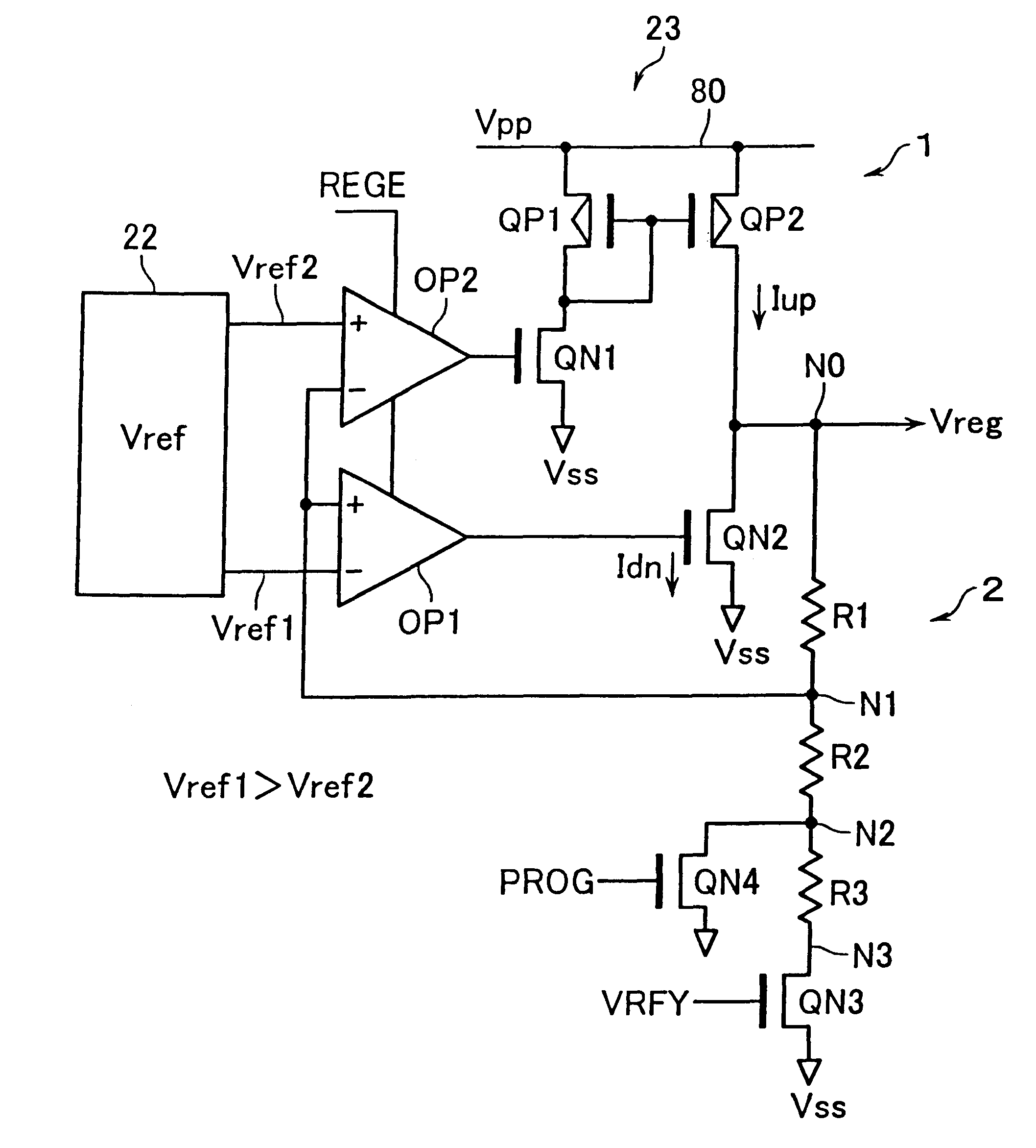
As shown in FIG. 1, the bitlines BL of the memory cell array 11 are ...


PUM


Abstract

A semiconductor device with a voltage regulator is disclosed. The voltage regulator includes: a driver including pull-up and pull-down transistors serially connected between an output node of an internal voltage generation circuit and a reference potential terminal, for outputting a regulated voltage at its regulated voltage output node corresponding to the connection node of the pull-up and pull-down transistors; a voltage divider circuit for subdividing the regulated voltage output to the regulated voltage output node; a first operational amplifier for controlling current drivability of the pull-down transistor in accordance with a difference between a first reference voltage and a divided output of the voltage divider circuit; and a second operational amplifier for controlling current drivability of the pull-up transistor in accordance with a difference between a second reference voltage and the divided output of the voltage divider circuit in such a way as to vary in a reverse direction to the current drivability of the pull-down transistor.

Description

This application is based on and claims the benefit of priority from the prior Japanese Patent Application No. 2001-052588, filed on Feb. 27, 2001, the entire contents of which are incorporated herein by reference.1. Field of the InventionThis invention relates generally to a semiconductor device having a voltage regulator for output of a regulated voltage that is variable in response to an output voltage of an internal voltage generation circuit.2. Description of the Related ArtPrior known electrically rewritable non-volatile semiconductor memory devices include electrically erasable programmable read-only memory (EEPROM) chips, also known as "Flash" memories in the semiconductor device art. Currently available Flash EEPROM chips come with an array of rows and columns of nonvolatile memory cells, each of which is typically formed of a metal insulator semiconductor field effect transistor (MISFET) of the so-called "stack gate" structure with a floating gate and a control gate being ...

Claims


Application Information

Patent Timeline
Patent Type & Authority Patents(United States)
IPC IPC(8): G11C5/14G11C8/08G11C8/00G11C16/08G11C16/06G11C16/30G05F1/56G05F1/618H01L21/822H01L27/04
CPCG11C5/147G11C8/08G11C16/08G11C16/30
Inventor TANZAWA, TORU
Owner KIOXIA CORP
Why Eureka
Try Eureka