

Delay locked loop circuit and method having adjustable locking resolution
a technology of locking resolution and loop circuit, which is applied in the direction of digital storage, pulse automatic control, instruments, etc., can solve the problems of deteriorating high frequency operation of semiconductor integrated circuit, and affecting the stability of the circui
- Summary
- Abstract
- Description
- Claims
- Application Information
AI Technical Summary
Problems solved by technology
Method used
Image

Examples
first embodiment
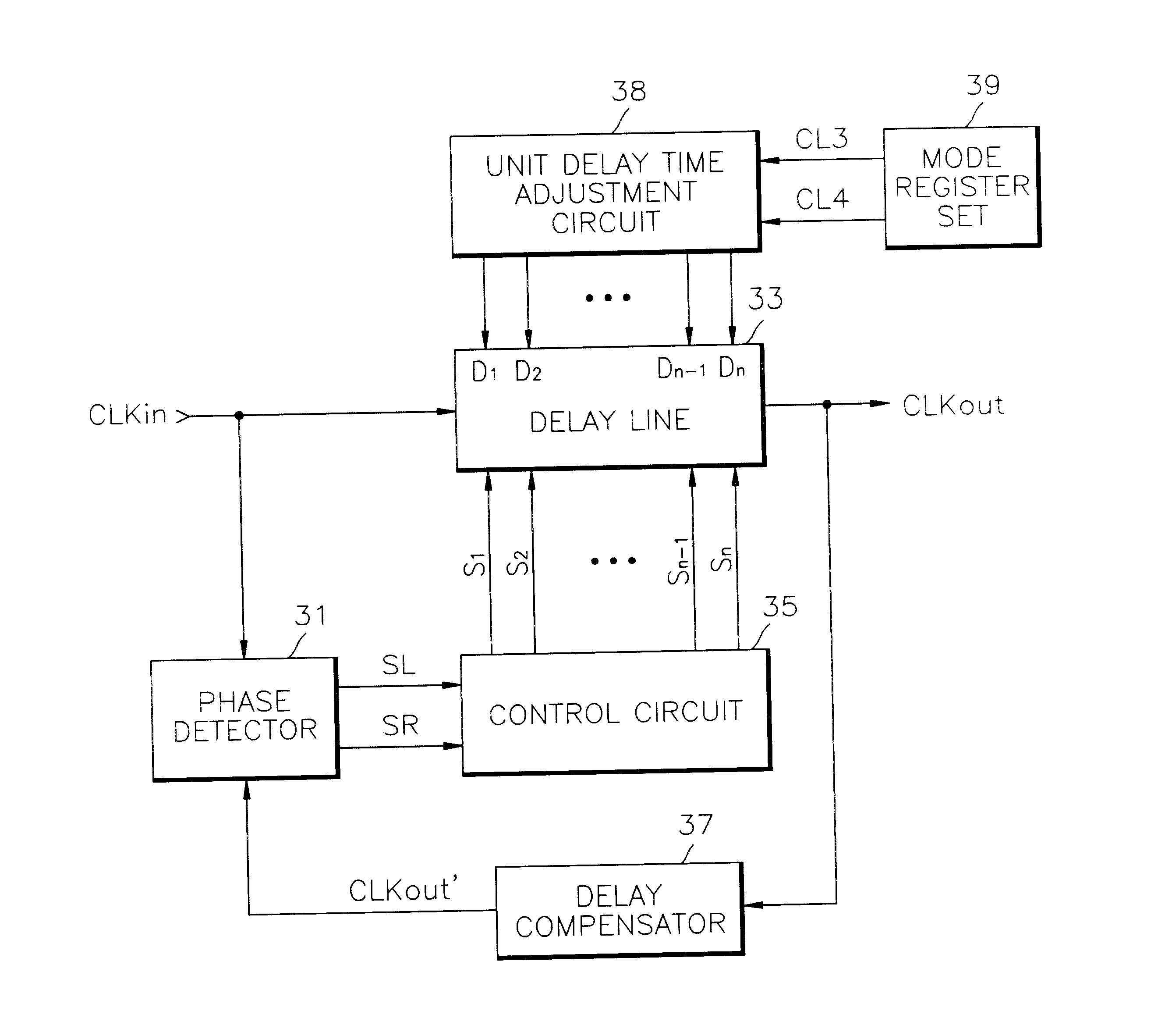
FIG. 3 is a block diagram of a DLL circuit according to the present invention. The DLL circuit of this embodiment includes a phase detector 31, a delay line 33, a control circuit 35, a delay compensator 37, a unit delay time adjustment circuit 38, and a Mode register set 39.
As shown, an external clock signal CLKin is delayed by the delay line 33 to produce an internal clock signal CLKout which is delayed relative to the external clock signal CLKin. The delay line 33 includes a plurality of unit delay circuits (not shown) which are selectively enabled in response to respective control signals S1 through Sn. The unit delay circuits are cascaded (connected in series) such that an amount of delay of the internal clock signal CLKout relative to the external clock signal CLKin depends on a number of the unit delay circuits which are effectively enabled by the control signals S1 through Sn.
The phase detector 31 receives a signal CLKout' (which is the internal signal CLKout after passing th...
second embodiment
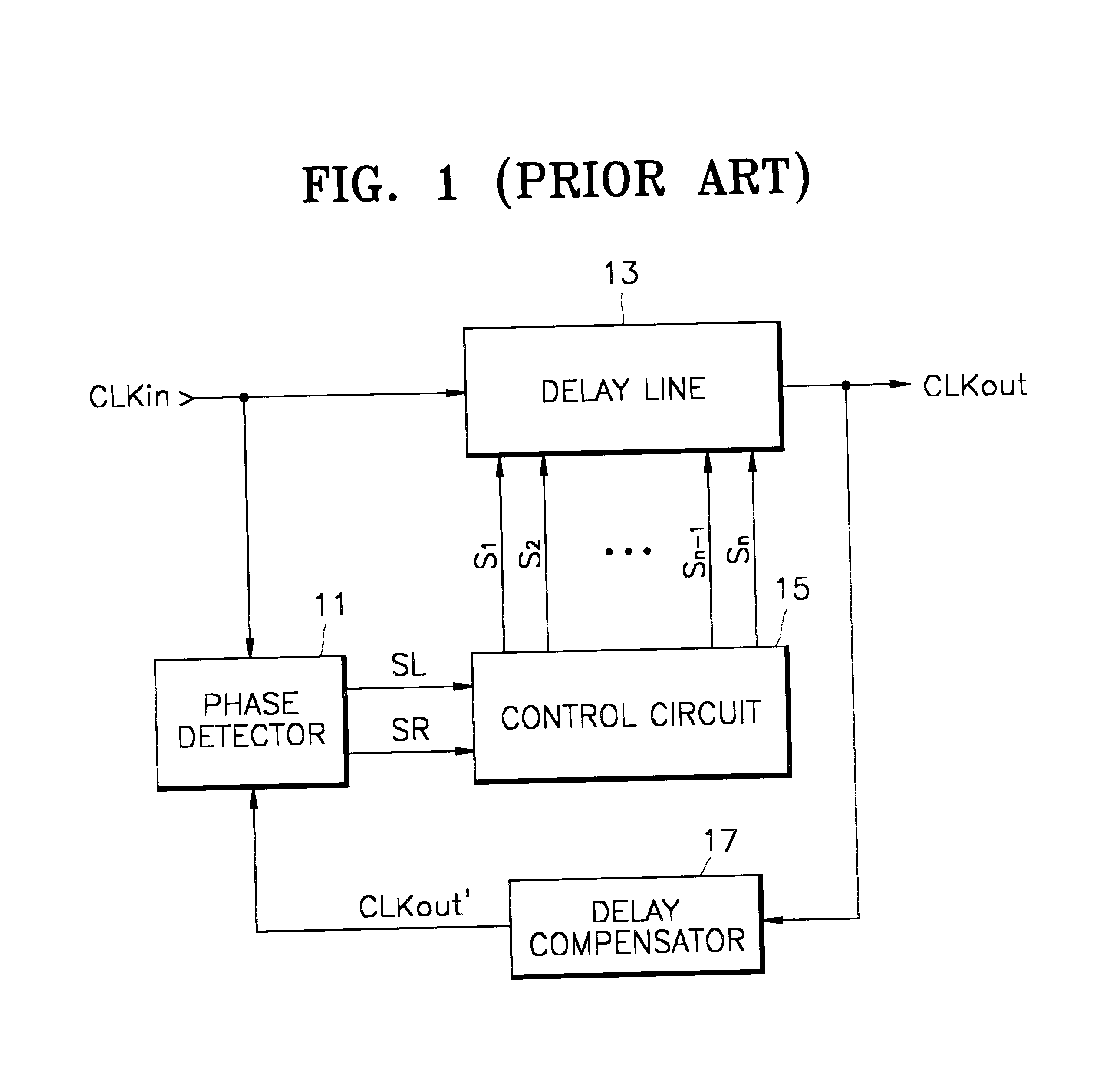
FIG. 7 is a block diagram of a DLL circuit according to the present invention. The DLL circuit of this embodiment includes a phase detector 71, a delay line 73, a control circuit 75, a delay compensator 77, and a Mode register set 79.
As shown, an external clock signal CLKin is delayed by the delay line 73 to produce an internal clock signal CLKout which is delayed relative to the external clock signal CLKin. The delay line 73 includes a plurality of unit delay circuits (not shown) which are selectively made operational in response to respective control signals S1 through Sn. The unit delay circuits are cascaded (connected in series) such that an amount of delay of the internal clock signal CLKout relative to the external clock signal CLKin depends on a number of the unit delay circuits which are enabled by the control signals S1 through Sn.
The phase detector 71 receives a signal CLKout' (which is the internal signal CLKout after passing through the delay compensator 77) and the exte...
PUM
 Abstract
Description
Claims
Application Information