Noncontact interface circuit and method for clamping supply voltage therein

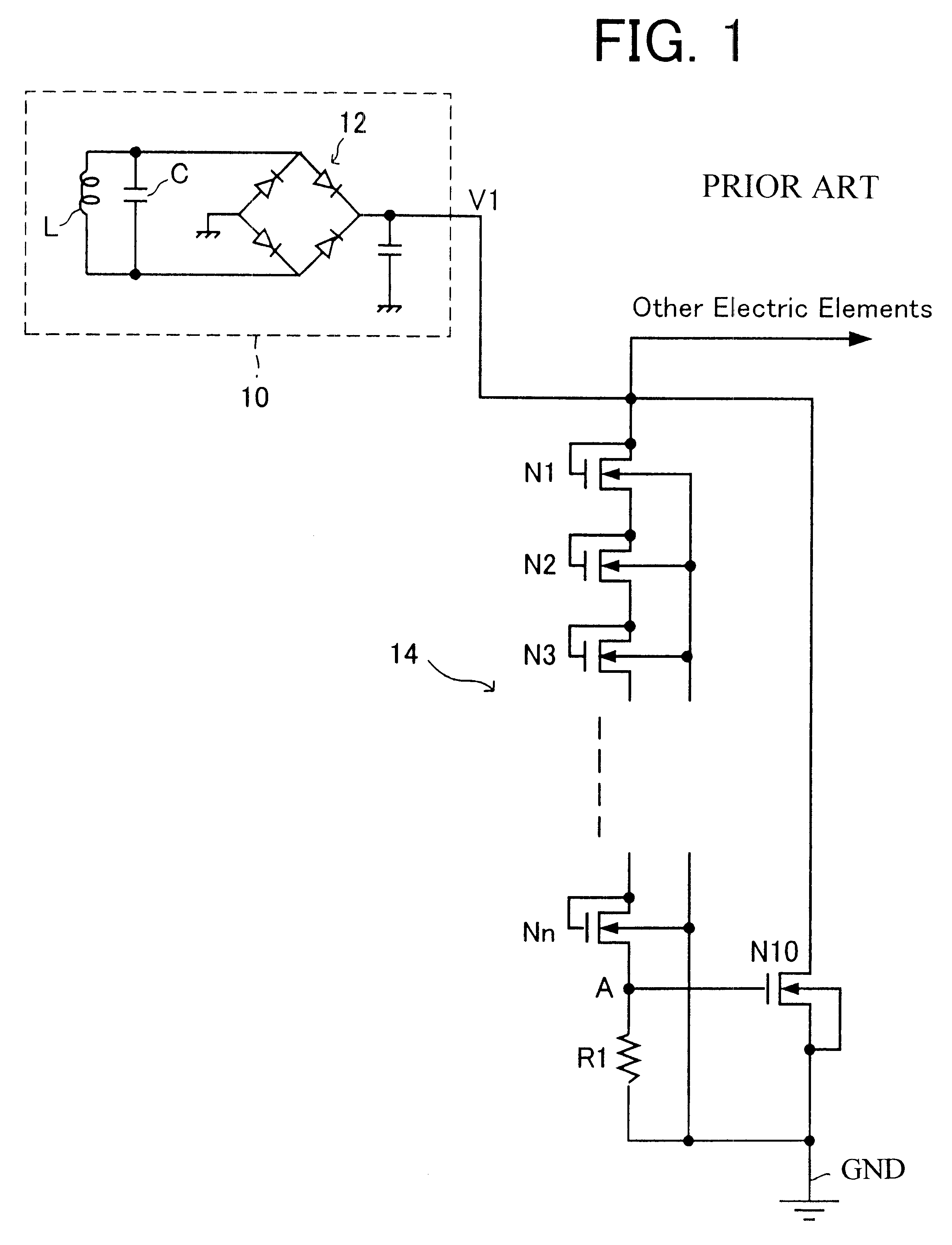
a non-contact, interface circuit technology, applied in the direction of pulse technique, process and machine control, instruments, etc., can solve the problems of reducing yield rate, circuit elements in the ic card may be damaged, uneven threshold voltage of the n-type mos transistor n1 to nn,

Inactive Publication Date: 2003-10-07
RAKUTEN INC
View PDF8 Cites 31 Cited by
  • Summary
  • Abstract
  • Description
  • Claims
  • Application Information

AI Technical Summary

Benefits of technology

Accordingly, an object of the present invention is to provide a contactless (noncontact) interface circuit that starts a clamping operation of a supply voltage accurately at an appropriate timing.
Another object of the present invention is to provide a method for clamping a supply voltage, in which a clamping operation starts accurately at an appropriate timing.

Problems solved by technology

The threshold voltage of the N type MOS transistors N1 to Nn are uneven due to structure unevenness thereof.
As a result, when the threshold voltage of the N type MOS transistors N1 to Nn shifts too low a value the clamping operation starts even if the a supply voltage is not yet high enough, so that undesirable electric current flows therethrough.
As a result, the circuit elements in the IC card may be damaged.
It is possible to reject defective IC cards in which N type MOS transistors N1 to Nn have uneven threshold voltages, however, the yield rate is decreased because many IC cards may be rejected.

Method used


Image

  • Noncontact interface circuit and method for clamping supply voltage therein
  • Noncontact interface circuit and method for clamping supply voltage therein
  • Noncontact interface circuit and method for clamping supply voltage therein

Examples


third embodiment

FIG. 7 shows a part of an IC card according to a third preferred embodiment of the present invention. In FIG. 7, the same or corresponding elements to those in the first and second preferred embodiment are represented by the same reference numerals and symbols; and the same description is not repeated. a clamp circuit further includes a capacitor C1, which is connected between node B and node C.

As shown in FIG. 8, when the supply voltage V1 exceeds (gets over) the clamp voltage V0, the transistor N10 turns on in response to an output signal of the differential amplifier A1, which is applied to the node B. When the transistor N10 turns on, the supply voltage V1 is maintained to be identical to the clamp voltage V0 in the clamping operation or clamping mode. The capacitor C1 is connected between the nodes B and C, so that it takes a time "t" until the transistor N10 turns on. The time "t" depends on the capacity of the capacitor C1. After the time "t", made by the capacitor C1, the t...

fifth embodiment

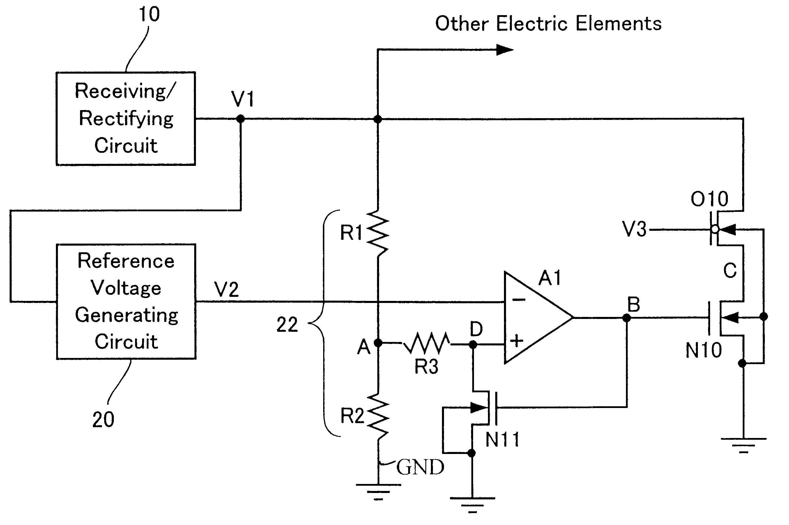
FIG. 11 shows a part of an IC card according to a fifth preferred embodiment of the present invention. The fifth preferred embodiment is similar to the above described fourth preferred embodiment, and the same or corresponding elements to those in the above described embodiment are represented by the same reference numerals and symbols; and the same description is not repeated. According to the fifth preferred embodiment, a clamp circuit includes a capacitor C1 between the node B and node C. The clamp circuit of the fifth preferred embodiment is provided with the feature (capacitor C1) of the third preferred embodiment and the feature (auxiliary resistor R3 and N type MOS transistor N11) of the fourth preferred embodiment. Accordingly, the operation of the fifth embodiment includes both the operations of the third and fourth preferred embodiment, as shown in FIG. 12.

When the supply voltage V1 increases and exceeds the clamp voltage V0, the transistor N10 turns on in response to the ...


PUM


Abstract

A supply voltage is divided to provide a divided supply voltage. The divided supply voltage is compared with the reference voltage. The supply voltage is controlled based on the result of comparison so that the supply voltage does not exceed a predetermined breakdown voltage.

Description

This application claims the priority of Application No. 2000-22218, filed Jan. 31, 2000 in Japan, the subject matter of which is incorporated herein by reference.The present invention relates to a contactless (noncontact) interface circuit for contactless data transmission and a method for clamping a supply voltage; and more particularly to, a contactless (noncontact) interface circuit that controls a supply voltage for application to an internal circuit so that the supply voltage does not exceed a breakdown voltage.In recent years, contactless (noncontact) IC cards have been developed and put to use. A conventional IC card includes, as shown in FIG. 1, a receiving / rectifying circuit, which receives voltage (alternating voltage) supplied from a coil in a coupler and rectifies the received voltage. The conventional IC card further includes a high supply voltage clamp circuit, which controls a power-supply voltage generated by the receiving / rectifying circuit so that the supply voltag...

Claims


Application Information

Patent Timeline
Patent Type & Authority Patents(United States)
IPC IPC(8): G05F1/10G05F1/575H02J5/00G06K19/07G06K17/00H03K5/007H03K5/08
CPCH02J5/005G05F1/575H02J50/12H02J50/10
Inventor TAKABAYASHI, YASUTAKA
Owner RAKUTEN INC
Why Eureka
Try Eureka