Method and apparatus for embedded substrate and system status monitoring

a technology of embedded substrates and monitoring methods, applied in semiconductor/solid-state device testing/measurement, instruments, material analysis, etc., can solve problems such as increased processing costs, defective devices, and increased impact of contamination

Inactive Publication Date: 2003-10-07
APPLIED MATERIALS INC
View PDF65 Cites 100 Cited by
  • Summary
  • Abstract
  • Description
  • Claims
  • Application Information

AI Technical Summary

Problems solved by technology

Sources of contamination include wear from mechanical motion, degradation of seals, contaminated gases, other contaminated substrates, flaking of deposits from processing chambers, nucleation of reactive gases, condensation during chamber pumpdown, arcing in plasma chambers and so forth.
Such sources of contamination produce particles that contact the substrates and can result in defective devices.
As the geometries of device features shrink, the impact of contamination increases.
Another situation which can cause increased processing costs is improper substrate routing in the chip manufacturing facility.
Occasionally, a substrate may be improperly routed to a process chamber where the processing conditions cause a volatile reaction, thereby damaging the substrate and / or the processing chamber.
Processing this substrate in the PVD chamber is known to cause severe damage to the chamber, resulting in substantial repair and / or replacement costs.
Because current processing systems are not equipped to prevent misrouting, the cost of ownership is increased.
Thus, production flow is effectively disrupted during transfer and inspection of the substrates.
Consequently, conventional metrology inspection methods can drastically increase overhead time associated with chip manufacturing.
Further, because such an inspection method is conducive only to periodic sampling due to the negative impact on throughput, many contaminated substrates can be processed without inspection resulting in fabrication of defective devices.
Problems are compounded in cases where the substrates are redistributed from a given batch making it difficult to trace back to the contaminating source.
Current methods of calibration negatively impact throughput because the production must be halted in order to perform the calibration.
Degradation usually goes undetected until a catastrophic failure occurs.
The presence of such contamination indicates that the backsides of substrates are being scratched during a substrate handling step or the accumulation of processing byproduct.
Heretofore, however, no such integral devices or methods have been known to exist in processing systems.
Another disadvantage with conventional inspection systems is the prohibitive cost of the systems.
Current systems are typically expensive stand-alone platforms that occupy clean-room space.
As a result of the large area, or "footprint," required by the stand-alone inspection platforms, the cost of owning and operating such a system is high.
With regard to particle detection, the cost is further increased because of the electro-optics equipment utilized.
This equipment is configured to produce high-resolution detection of small-scale particles and requires high-fidelity mechanisms, which are expensive to operate.
Additionally, considerations of reduced throughput described above further increase the cost of conventional inspection systems.
A subsequent determination that a substrate is under-processed typically results in the substrate being discarded because the time involved in returning the substrate for additional processing and possible growth of a native oxide is cost prohibitive.
Given the amount of data involved, even subtle changes on the substrate's surface can cause substantial changes to the specular and / or scattering signature.

Method used


Image

  • Method and apparatus for embedded substrate and system status monitoring
  • Method and apparatus for embedded substrate and system status monitoring
  • Method and apparatus for embedded substrate and system status monitoring

Examples


Embodiment Construction

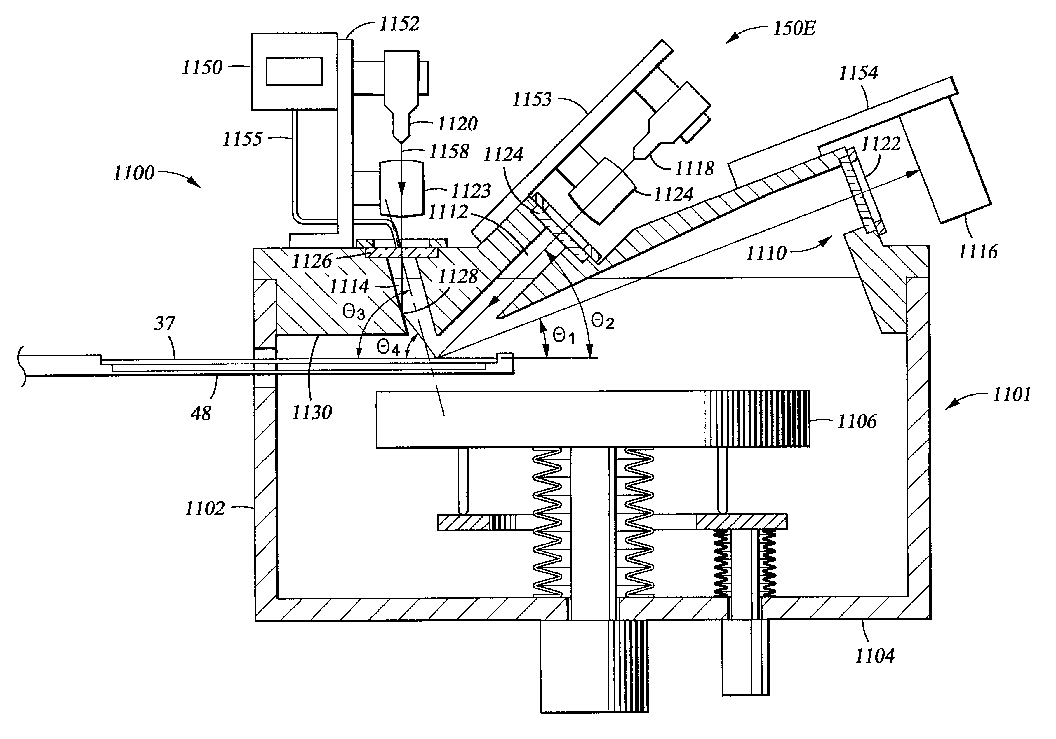
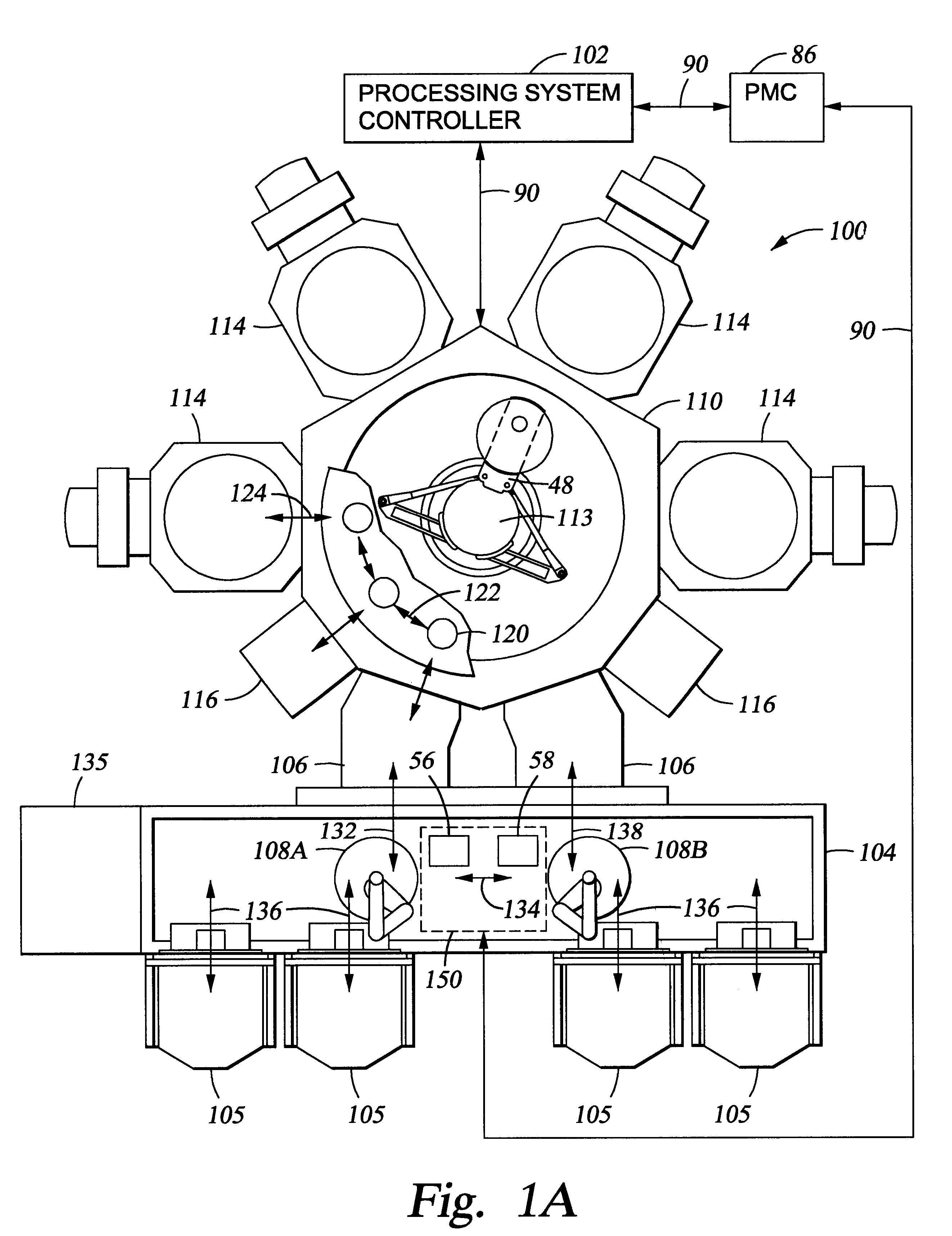
Substrates were processed on a Centura system equipped with a DPS Metal Etch Chamber and an ASP strip / passivation chamber, both available from Applied Materials, Inc., located in Santa Clara, Calif. After etch and strip processing, this hot substrate is cooled to near room temperature in a cooldown chamber which includes an apparatus system according to an embodiment of the invention.

Processed substrates consisted of EPIC-generated substrates, utilizing Applied Materials equipment for all steps except for lithography. The photoresist / metal stack on the substrates was: 8000 A DUV photoresist / 250 A TiN ARC / 5500 A Al--Cu0.5% / 250 A TiN / 200 A Ti / 3000 A thermal oxide. A dense pattern covered about 50% of the substrate, consisting of 0.25 .mu.m lines / spaces.

All substrates were etched using a typical recipe. This etched the metal stack entirely, leaving approximately 5200 A of photoresist on most patterned features (3700 A at the shoulder of patterned lines).

As chip geometries shrink, a gre...


PUM

PropertyMeasurementUnit
timeaaaaaaaaaa
widthaaaaaaaaaa
widthaaaaaaaaaa

Abstract

The present invention generally provides an apparatus and a method for inspecting a substrate in a processing system. One embodiment provides a substrate inspection apparatus, comprising a vacuum chamber lid, the lid comprising a body defining at least three ports located to provide a field of view to a common area on a substrate transfer plane and light management system.

Description

1. Field of the InventionThe invention relates to inspection methods and apparatus. More particularly, the invention relates to a method and apparatus for inspection of substrates to identify process and handling related defects and conditions.2. Background of the Related ArtA chip manufacturing facility is composed of a broad spectrum of technologies. Cassettes containing semiconductor substrates are routed to various stations in the facility where they are either processed or inspected.Semiconductor processing generally involves the deposition of material onto and removal ("etching") of material from substrates. Typical processes include chemical vapor deposition (CVD), physical vapor deposition (PVD), electroplating, chemical mechanical planorization (CMP) etching and others. During the processing and handling of substrates, the substrates undergo various structural and chemical changes. Illustrative changes include the thickness of layers disposed on the substrate, the material ...

Claims


Application Information

Patent Timeline
Patent Type & Authority Patents(United States)
IPC IPC(8): G01N21/956G01N21/88G01N21/95G01N21/94H01L21/00H01L21/66
CPCG01N21/94G01N21/9501H01L21/67276H01L21/67253G01N21/956G01N2021/4704
Inventor HUNTER, REGINALD
Owner APPLIED MATERIALS INC
Why Eureka
Try Eureka