Method of filling contact hole of semiconductor device

a technology of contact hole and semiconductor device, which is applied in the direction of semiconductor devices, electrical equipment, basic electric elements, etc., can solve the problems of affecting the electrical properties of the substrate, and forming a damaged layer

Inactive Publication Date: 2003-10-28
SAMSUNG ELECTRONICS CO LTD
View PDF11 Cites 67 Cited by
  • Summary
  • Abstract
  • Description
  • Claims
  • Application Information

AI Technical Summary

Problems solved by technology

However, such etching process can also induce an ion bombardment effect which in turn results in lattice defect or distortion with regard to the semiconductor substrate underlying the patterned material layer or polycrystalline silicon (polysilicon).
Due to the lattice defect or distortion, a damaged layer is formed on a semiconductor substrate exposed by the dry etch.
The existence of the damaged layer thus formed may change the electrical properties of the substrate, for example, deteriorate the electrical conductivity.
There are disadvantages among

Method used


Image

  • Method of filling contact hole of semiconductor device
  • Method of filling contact hole of semiconductor device
  • Method of filling contact hole of semiconductor device

Examples


Embodiment Construction

The present invention now will be described more fully with reference to the accompanying drawings, in which preferred embodiments of the invention are shown. This invention may, however, be embodied in many different forms and should not be construed as being limited to the embodiments set forth herein; rather, these embodiments are provided so that this disclosure will be thorough and complete, and will fully convey the concept of the invention to those skilled in the art. In the drawings, the thickness of layers is exaggerated for clarity, and the same reference numerals in different drawings represent the same element. Further, it will be understood that when a layer is referred to as being "on" another layer or substrate, it can be directly on the other layer or substrate, or intervening layers may also be present.

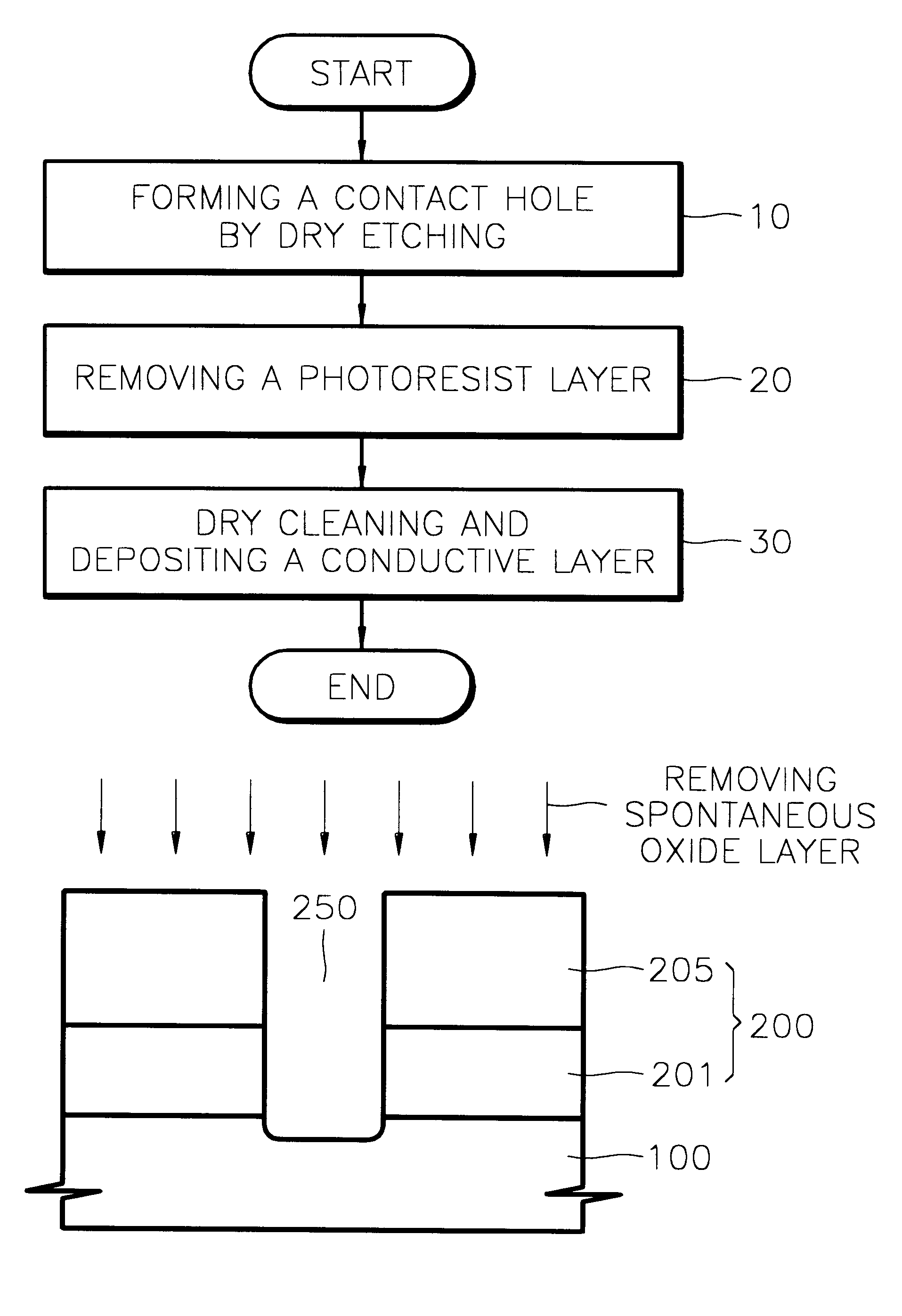
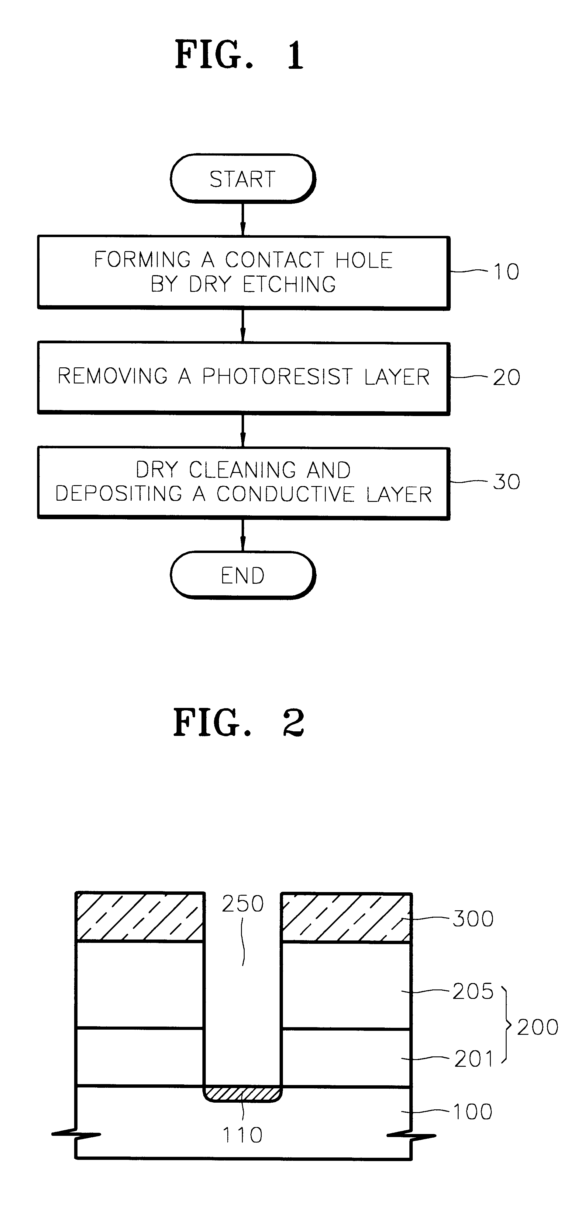
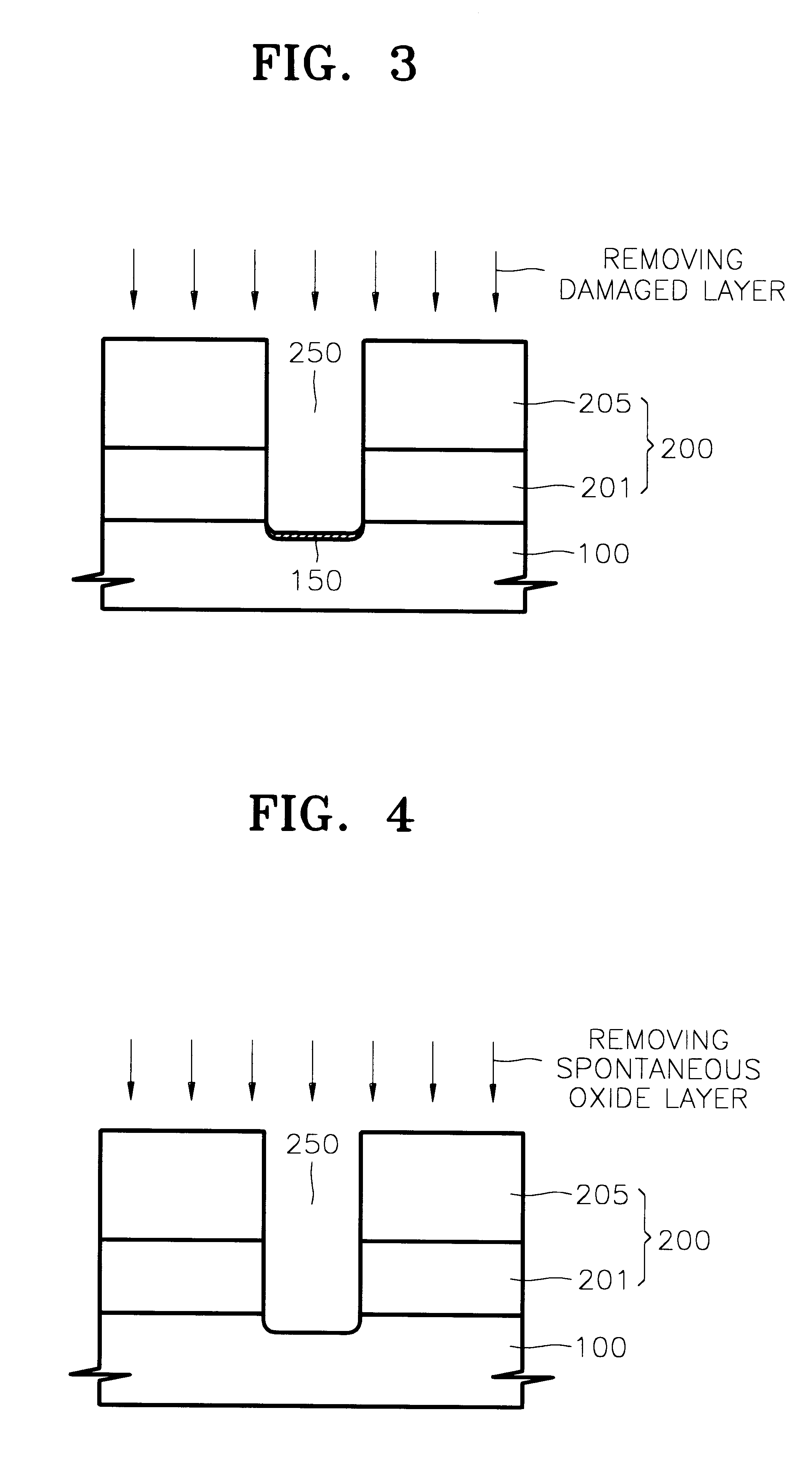
FIG. 1 is a flowchart showing a method for filling a contact hole of a semiconductor device according to a preferred embodiment of the present invention.

A preferred e...


PUM


Abstract

A method of filling a contact hole of a semiconductor device preceded by dry cleaning for removing a damaged layer resulting from dry etching is provided. The method includes selectively exposing an underlying material layer by a dry etch and dry cleaning including passing plasma excited from a source gas over the exposed underlying material layer to remove the damaged layer formed from the dry etch. Subsequently, an electrically conductive layer with which to fill the contact hole is formed. The formation of the electrically conductive layer is performed in a separate chamber connected sequentially to a chamber for performing the dry cleaning to prevent the exposed underlying material layer inside the dry cleaned contact hole from being exposed to a source of contamination.

Description

1. Field of the InventionThe present invention relates to fabrication of a semiconductor device and more particularly, to a method of filling a contact hole of a semiconductor device using a dry cleaning process, and to a method of removing a damaged layer resulting from a prior dry etching process.2. Description of Related ArtAs integration density of semiconductor devices increases, cleaning processes therefor become increasingly important. For instance, following a dry etching process for forming a contact hole, it is important that a proper process of cleaning the surface of a semiconductor substrate exposed by the contact hole or the sidewalls thereof prior to a process for filling the contact hole is utilized. Dry etching for patterning is performed in such a way that reactive ions contained in plasma are accelerated using a voltage difference to etch material layers and the like on a semiconductor substrate. Such dry etching process has increased in popularity as the feature ...

Claims


Application Information

Patent Timeline
IPC IPC(8): H01L21/768H01L21/02H01L21/311H01L21/70H01L21/306H01L21/28H01L21/304H01L21/302
CPCH01L21/02063H01L21/76877H01L21/76814H01L21/31116H01L21/02046H01L21/28
Inventor CHANG, KYU-HWANKO, YONG-SUNSONG, CHANG-LYONGCHONG, SEUNG-PIL
Owner SAMSUNG ELECTRONICS CO LTD
Why Eureka
Try Eureka