Method for inducing controlled cleavage of polycrystalline silicon rod

a polycrystalline silicon and rod technology, applied in the field of methods, can solve the problems of rod breakage during processing, large damage and down time of crystal growing equipment, and single crystal silicon growers have difficulty in obtaining good yield

Inactive Publication Date: 2004-01-13
REC SILICON
View PDF3 Cites 15 Cited by
  • Summary
  • Abstract
  • Description
  • Claims
  • Application Information

AI Technical Summary

Benefits of technology

The present invention relates to improving the yield of a polycrystalline silicon production system by increasing the useable length of polycrystalline silicon rods produced.
Thus, by inducing a flaw in a filament in the region of the filament-bridge connection, it is possible to cause the resulting rod to fracture generally perpendicularly to the axis of the rod at an elevation above the elevation of the bottom of the spall that otherwise likely would occur.

Problems solved by technology

In addition, many CZ single crystal silicon growers have difficulty obtaining good yield if they add more than 10-20% of the total weight of the charge as granular polycrystalline silicon.
Cracks can cause the rods to break during processing due to thermal as well as internal stresses.
Such breakage can cause extensive damage and down time to the crystal growing equipment.
Spalls, depending on size and location, are also detrimental to the process.
This is due to the potential for cracks to be associated with the spalling.
In addition, the loss of mass associated with spalls can impact the quantity of single crystal produced.
Rod spalls lead to variability in the rod length / mass ratios that must be compensated for during processing, which can lead to reduced productivity.
Unfortunately, at each filament-bridge junction region there is generated a large amount of radiant energy that is exchanged between the filament and the bridge.
This results in a large amount of induced stress in the rod.
This stress can become great enough to cause the rods to fracture in this region upon cooling.
Thus in many cases, the rod can no longer be processed for the FZ process and may not be useable for the CR rod process.
Spalling of the rods in the reactor can greatly impact this yield.
This excessive temperature causes induced stresses which, upon cooling, can result in fracturing or spalling of the grown polycrystalline silicon rod 10.

Method used


Image

  • Method for inducing controlled cleavage of polycrystalline silicon rod
  • Method for inducing controlled cleavage of polycrystalline silicon rod
  • Method for inducing controlled cleavage of polycrystalline silicon rod

Examples


Embodiment Construction

It was desired to grow 138 mm diameter rods approximately 1550 mm in length in a Siemens reactor using silane as the source gas.

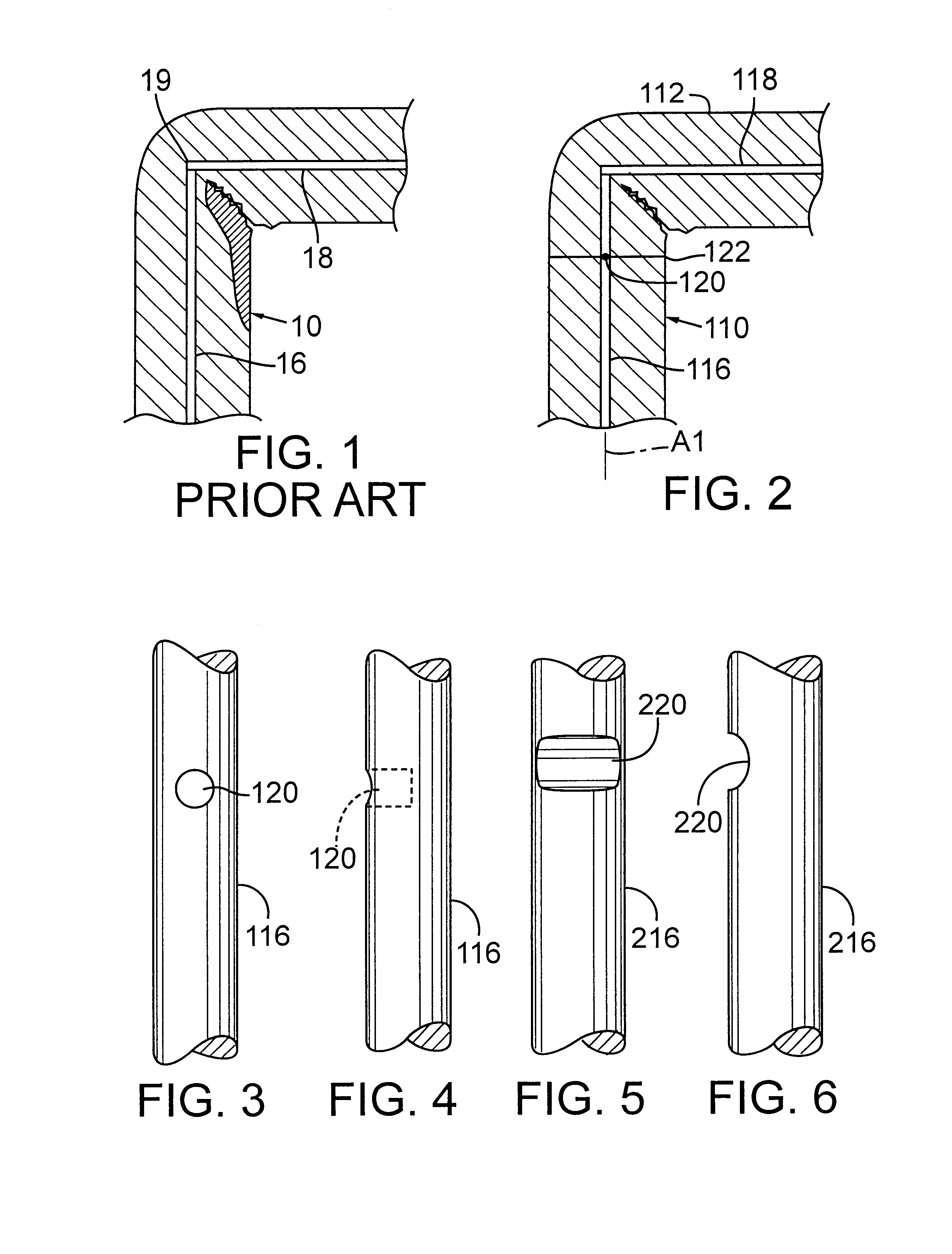
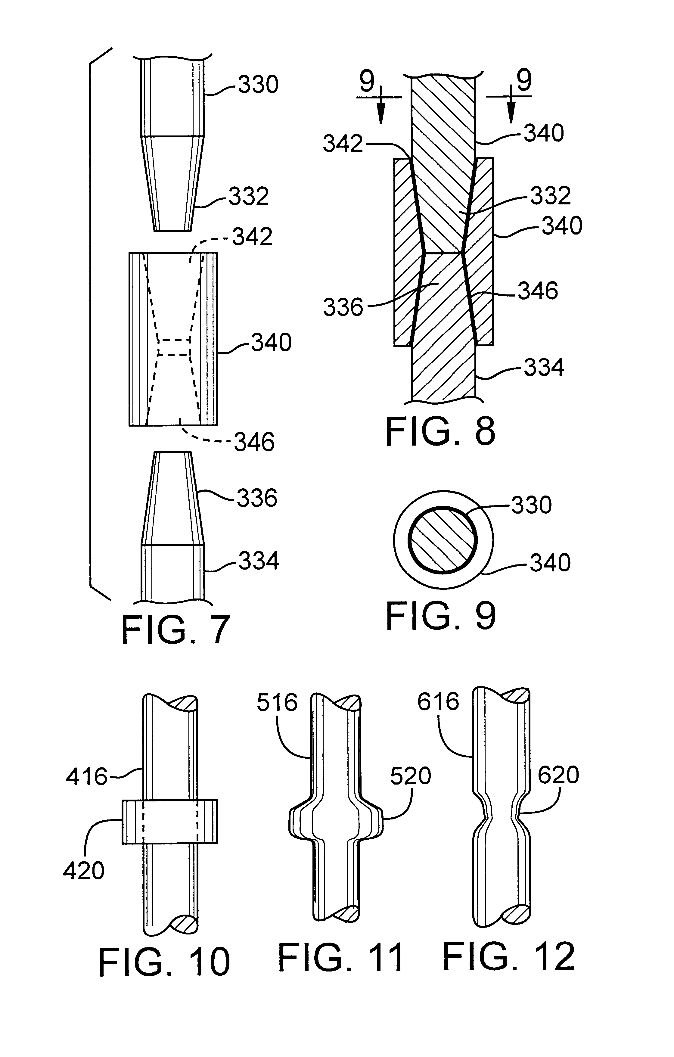
In order to make the resulting rods fracture satisfactorily at a specific location, a 0.5 mm hole was machined into each of several 7-mm starter rods that were 2200 mm long.

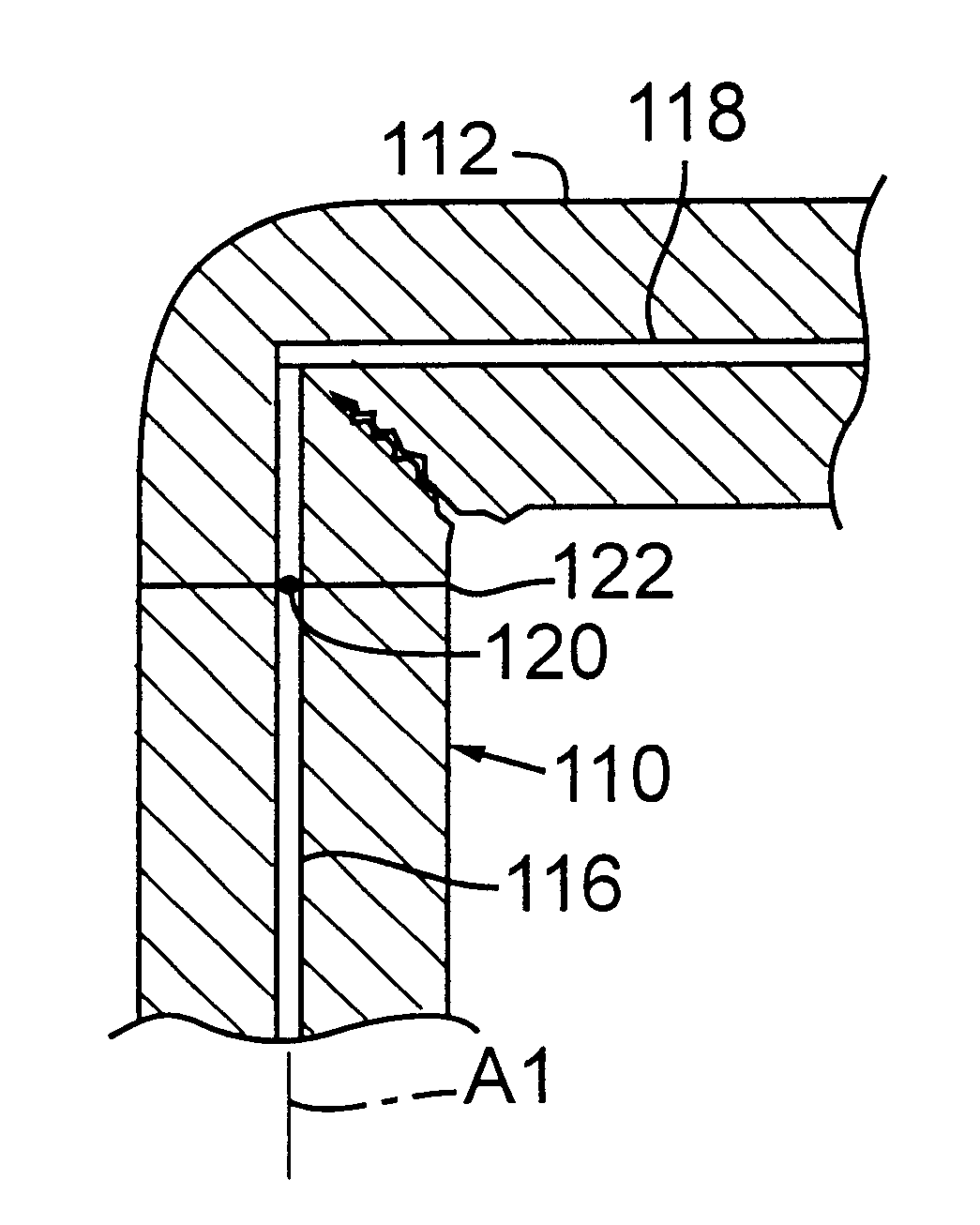
The hole was approximately 2.5 mm in depth. For this test, the flaw was located 100 mm below the bridge end of each starter rod.

After the growth cycle, all the resulting 138-mm diameter rods broke cleanly. In nearly all cases, the fracture plane was directly through the flaw. Among fifteen rods that were grown on filaments having the induced flaw, there was a single spall 240 nm in length.

In comparison, seventeen rods grown on similar filaments, but without induced flaws, had ten spalls averaging 224 mm in length with a standard deviation of 253 mm. Available rod length thus was increased by an average of 72 mm when using flawed filaments.

It will be apparent to those having ordinary skil...


PUM

PropertyMeasurementUnit
lengthaaaaaaaaaa
weightaaaaaaaaaa
lengthaaaaaaaaaa

Abstract

To avoid problems associated with the formation of unwanted cracks and spalls during the growth of a polycrystalline silicon rod, a flaw is induced in a filament on which silicon will be deposited to produce a rod. The flaw causes the grown rod to have a cleavage plane such that the rod will break in a controlled manner at a desired location. The flaw can be placed at a location selected such that breakage at the cleavage plane will produce long rods and thereby improve the yield of the rod growing process. Such a flaw will also have the effect of minimizing useable rod length losses due to spalling.

Description

BACKGROUND AND SUMMARYThe present invention relates to improving the yield of a polycrystalline silicon production system by increasing the useable length of polycrystalline silicon rods produced.Polycrystalline silicon is a critical raw material for the electronics industry. It is the starting material for producing single crystal silicon ingots for the semiconductor industry. These ingots are produced either by the Czochralski (CZ) or Float Zone (FZ) method.In the CZ crystal pulling process, chunks of polycrystalline silicon are loaded into a quartz crucible. The chucks of polycrystalline silicon are random size varying from 14 inches in length. In order to maximize the packaging density of the polycrystalline silicon, polycrystalline chips, granules or short rod pieces may also be added to the quartz crucible to increase the packing density. The crucible is filled, loaded into the CZ furnace and the polycrystalline silicon is melted.Upon melting, due to interstices among the poly...

Claims


Application Information

Patent Timeline
Patent Type & Authority Patents(United States)
IPC IPC(8): C23C16/24C23C16/22C23C16/44
CPCC23C16/24C23C16/4418Y10T428/2913
Inventor KECK, DAVID W.OSBORNE, EDWARD W.KAMRUD, HALVOR
Owner REC SILICON
Why Eureka
Try Eureka