Circuit for processing trace information

a trace information and circuit technology, applied in the field of processing information, can solve the problems of difficult access to this information, sometimes destructive access to memory locations, and difficult debugging of these systems

Inactive Publication Date: 2004-01-27
RENESAS ELECTRONICS CORP
View PDF104 Cites 135 Cited by
  • Summary
  • Abstract
  • Description
  • Claims
  • Application Information

AI Technical Summary

Problems solved by technology

Because multiple modules and their communications occur internally to the chip, access to this information is generally difficult when problems occur in software or hardware.
Thus, debugging on these systems is not straightforward.
However, debugging an SOC generally involves intrusively monitoring one or more processor registers or memory locations.
Accesses to memory locations are sometimes destructive, and a data access to a location being read from a debugging tool may impede processor performance.
Similarly, accesses are generally performed over a system bus to the processor, memory, or other module, and may reduce available bandwidth over the system bus for performing general operations.
By slowing or pausing the processor, some types of errors may not be reproduced, and thus cannot be detected or corrected.
Further, accurate information may not be available altogether due to a high speed of the processor; information may be skewed or missing.
Howeve

Method used


Image

  • Circuit for processing trace information
  • Circuit for processing trace information
  • Circuit for processing trace information

Examples


Embodiment Construction

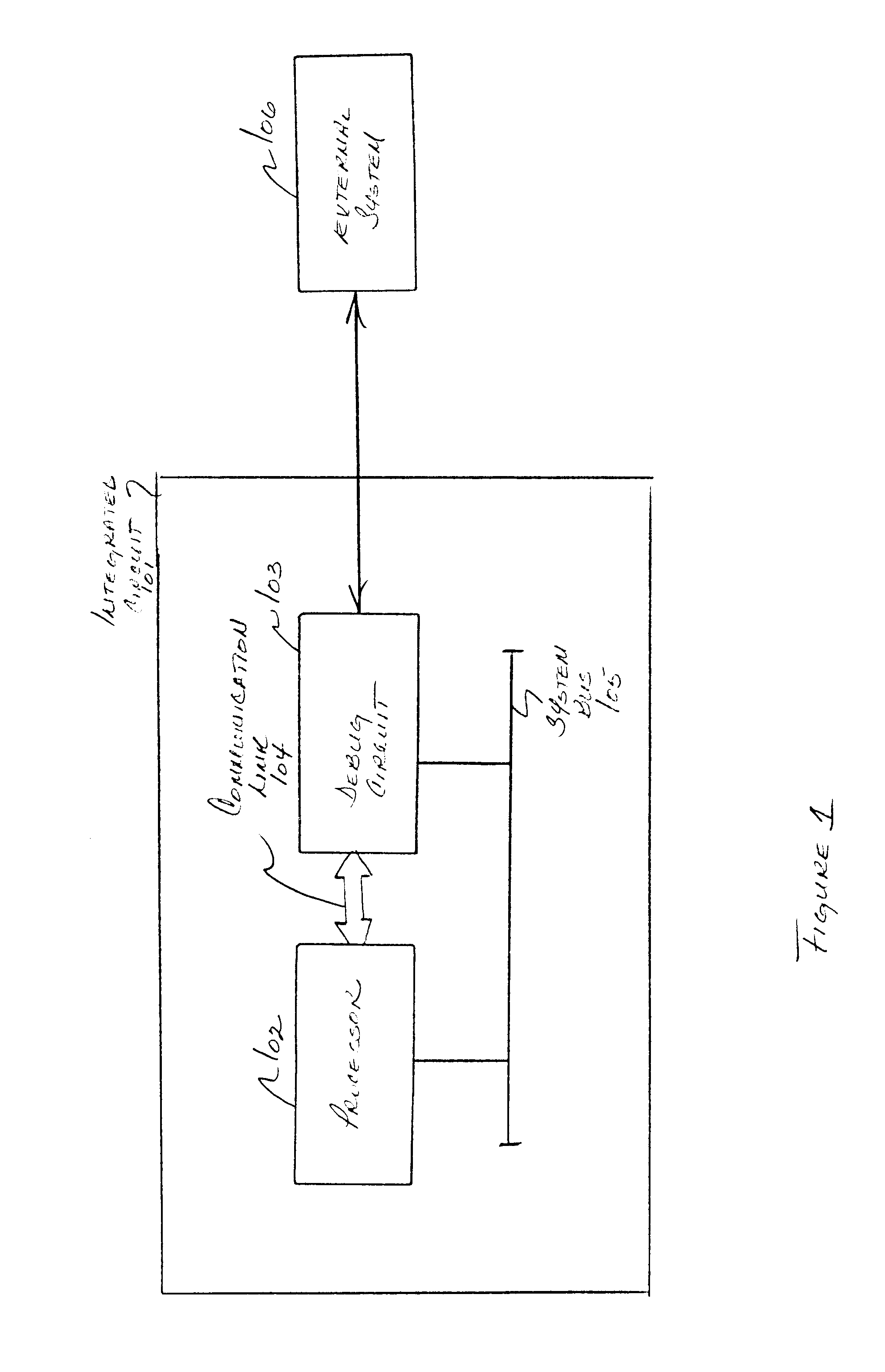
One embodiment of the invention is described with particularity with respect to FIG. 1. FIG. 1 shows a block diagram of an integrated circuit device 101, or system-on-chip (SOC) mentioned above. This circuit may include a processor 102 and debug circuit 103 interconnected by a system bus 105. System bus may be a conventional bus, packet switch, or other communication medium used to communicate operating information between modules of device 101. Operations such as reads, writes, swaps, and the like are typical operations that are performed between modules.

Processor 102 is a device which is adapted to read and execute program code in a one or more processor instructions, and to perform operations on data. Processor 102 may read data from a number of data sources, and write data to one or more data stores (not shown). These data stores may include Random Access Memory (RAM), a computer hard disc accessible through a hard disc controller, storage accessible over one or more communicati...


PUM


Abstract

A system for performing non-intrusive trace is provided which receives trace information from one or more processors. The trace system may be configured by a user to operate in various modes for flexibly storing or transmitting the trace information. The trace system includes a FIFO which is memory-mapped and is capable of being accessed without affecting processor performance. In one aspect, the trace system includes a trace buffer which receives trace information at an internal clock speed of the processor. In another embodiment, a compression protocol is provided for compressing trace messages on-chip prior to transmitting the messages to an external system or storing the messages in memory.

Description

BACKGROUND OF THE INVENTION1. Field of the InventionThe invention relates generally to performing trace on a system-on-chip (SOC), and more specifically, to processing information.2. Related ArtSystem-on-chip devices (SOCs) are well-known. These devices generally include a processor, one or more modules, bus interfaces, memory devices, and one or more system busses for communicating information. Because multiple modules and their communications occur internally to the chip, access to this information is generally difficult when problems occur in software or hardware. Thus, debugging on these systems is not straightforward. As a result of development of these SOCs, specialized debugging systems have been developed to monitor performance and trace information on the chip. Such systems typically include dedicated hardware or software such as a debug tool and debug software which accesses a processor through serial communications.However, debugging an SOC generally involves intrusively ...

Claims


Application Information

Patent Timeline
IPC IPC(8): G06F11/36G06F11/28G06F15/78
CPCG06F11/3636G06F11/3648
Inventor EDWARDS, DAVID ALANRICH, ANTHONY WILLIS
Owner RENESAS ELECTRONICS CORP
Why Eureka
Try Eureka