Microprocessor development systems

a microprocessor and development system technology, applied in the field of microprocessor development systems, can solve the problems of reducing the available program memory space for the application program, undesirable additional cost to provide memory resources for the implementation of the monitor program, and etc., to achieve the effect of simplifying memory access, reducing the need for complex logic, and being easy to us

Inactive Publication Date: 2003-06-03
AVAGO TECH WIRELESS IP SINGAPORE PTE
View PDF7 Cites 70 Cited by
  • Summary
  • Abstract
  • Description
  • Claims
  • Application Information

AI Technical Summary

Benefits of technology

In a deeply embedded application, such as a microprocessor which is a core element in an integrated circuit, it is an undesirable additional cost to provide memory resources to implement a monitor program. Access for debug software running on a deeply embedded microprocessor can be provided by means of a serial scan interface: that is by clocking data into and out of the system one bit at a time. In this serial scan method, known as ScanICE (trade mark), registers are provided throughout the microprocessor, coupled together in series to form a test scan chain which can be accessed by an external host to load test data into the scan chain and to read out the results. This permits the complete workings of the microprocessor to be observed. The main advantage of this serial scan method is that the test scan chain is used to retrieve the entire state of the microprocessor without the need for a monitor program to provide access to the internal registers. The serial scan method can be used to access memory mapped devices, slow memory, off-chip interfaces and so on. Specially designed hardware interfaces are designed into the system, which are controlled by the scan control logic. The scan control uses its complete access to all of the microprocessor's control signals to control the interface logic using successive scanned vectors. However, this method is very complex, requires a lot of additional logic and may be very difficult to use in mixed memory systems. Sometimes it is not economical or even possible to implement a hardware scan interface to a microprocessor peripheral in a system in this way.
A technique known as a "micromonitor" has been devised as a modification of the serial scan method to simplify memory access. In this a small program is downloaded into the processor's program memory to perform memory accesses using the normal microprocessor mode of operation (rather than using scan registers to control the memory interface). In this method, a quantity of program RAM and of data RAM is read by the debug system, and stored elsewhere, i.e. backed-up. A very small program is loaded, using serial scanning, into this available program RAM space after having read and backed up the previous contents. Using the available data RAM space as a transfer data buffer, the program is used to access the memory or peripheral by returning the microprocessor to its normal running state executing instructions at the addresses of the available quantity of program RAM. Once the data transfer is complete, the backed-up data and program RAM contents are loaded back into the quantity of RAM and execution can continue normally. Hence the need for complex logic is reduced. However, this method relies on there being some accessible program RAM which is writable, because it is still necessary to read portions of the microprocessor's data and program into the debugging system and to store them while the memory is used for the requirements of the micromonitor. Many embedded systems only contain ROM for program memory, so there is no possibility of downloading a micromonitor into normal RAM.

Problems solved by technology

The disadvantages of this method are that it requires program memory resources (either RAM or ROM) to be provided in the system to hold the monitor program.
If ROM is provided, this causes a reduction in the available program memory space for the application program.
In a deeply embedded application, such as a microprocessor which is a core element in an integrated circuit, it is an undesirable additional cost to provide memory resources to implement a monitor program.
However, this method is very complex, requires a lot of additional logic and may be very difficult to use in mixed memory systems.
Sometimes it is not economical or even possible to implement a hardware scan interface to a microprocessor peripheral in a system in this way.

Method used


Image

  • Microprocessor development systems
  • Microprocessor development systems
  • Microprocessor development systems

Examples


Embodiment Construction

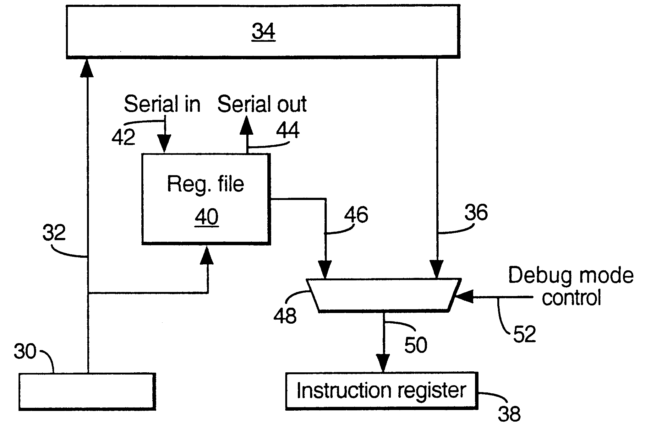
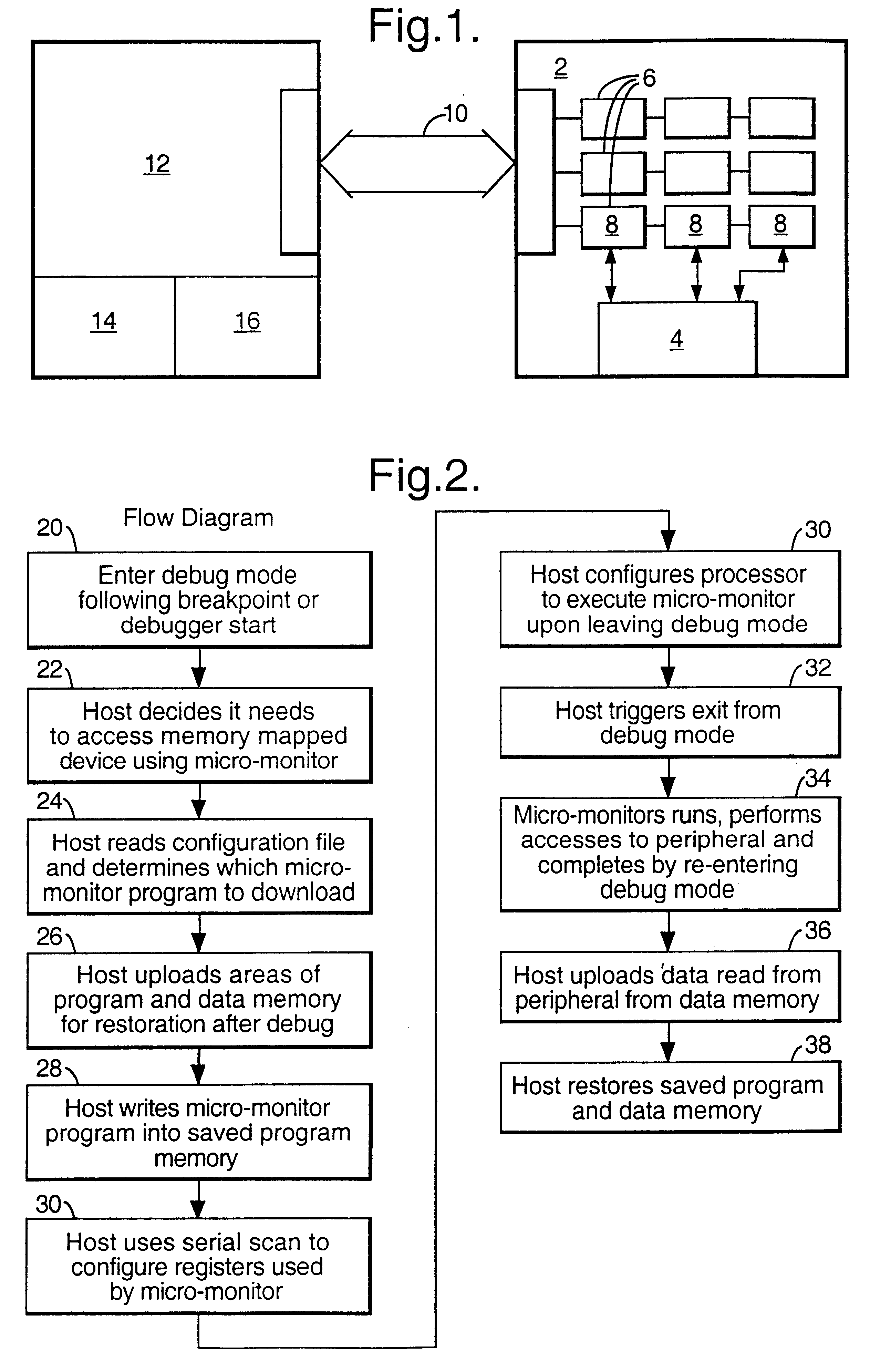
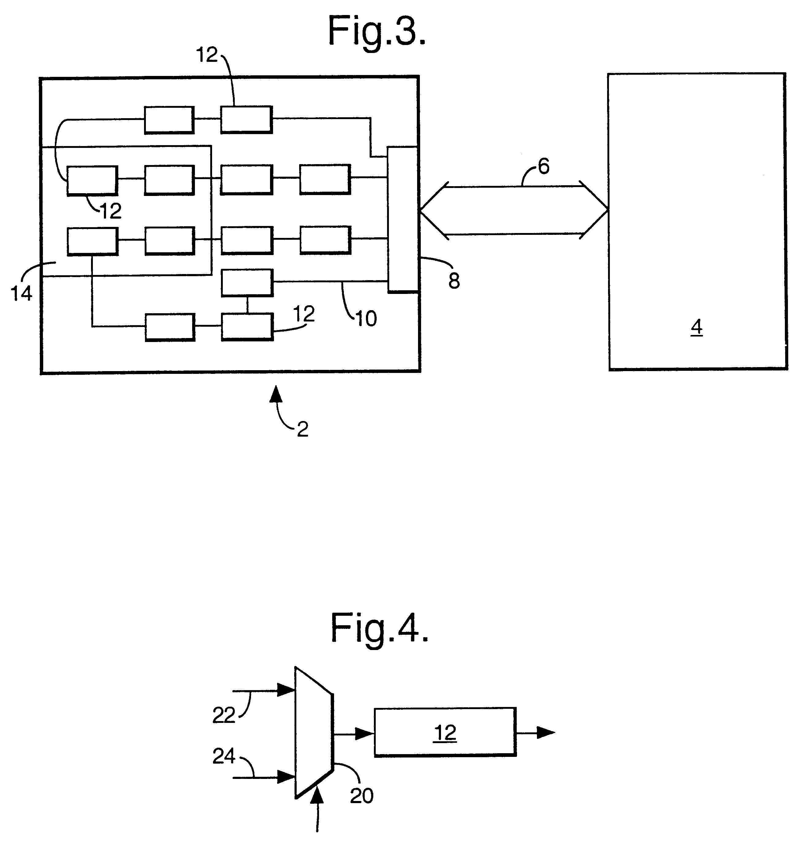
Referring to FIG. 1, there is shown a target processor 2 forming part of a deeply embedded application having an area of memory 4 and a series of scan chains 6 formed by coupling registers of the memory in series in the scan mode. Registers 8 of one scan chain are coupled to memory 4. The scan chains are connected to an interface 10 which is coupled to a host computer 12 and which permits a transfer of data and instructions during a debug or scan procedure. The host computer includes an area of memory 14 which includes a user-configurable file 16. In file 16 are stored data and monitor programs required for access of desired peripherals (not shown) by the target processor.

Referring now to FIG. 2, the method in accordance with the preferred embodiment of the invention is carried out as follows:

Upon entry into scanning (debug) mode as at 20, the host system (executing or operating under control of the debugger) scans data out of the target processor's scan chain and saves that informa...


PUM


Abstract

A procedure and processor are disclosed for avoiding lengthy delays in debug procedures during access by a memory mapped peripheral device. The processor includes in-circuit emulation means comprising one or more scan chains or serially connected registers for access by an external host computer system. The procedure comprises:a) the host computer system carrying out a debug procedure via said scan chains, and selectively interrupting such debug procedure for access to a peripheral memory mapped device;b) the host computer system writing into an area or memory of the processor a program for reading and/or writing data at a specified memory location; andc) the host computer system causing said processor to run said program, and then to return to said debug procedure.In another aspect, in order to permit small debugging programs to run, in serial scan in circuit emulation processes, on a processor in a deeply embedded application where no program RAM is provided, the processor includes one or more chains of serially connected registers coupled to interface means for access by an external host to enable a serial scan procedure to be carried out, one such chain including a set of serially coupled registers for storing one or more processor instructions read into a set of registers through the interface means, and the processor including address means, for addressing program memory, coupled to said set of registers for addressing the set of registers, and means for reading the processor instructions in the set of registers to an instruction resister of the processor.

Description

The present invention relates to microprocessor development systems.FIRST INVENTIONNowadays microprocessor systems are frequently implemented as deeply embedded application specific systems, having a microprocessor core and with stored software routines and / or designed to run specific software routines. In order to remove errors and debug the system designed, microprocessor development systems are employed, which allow a technique called in-circuit emulation or in-circuit debug to enable the hardware and software designs to be debugged together by giving access to the state of the microprocessor and the progress of execution of the software program running on the microprocessor. Typically, this is realised by a special program, sometimes called a debug monitor, which runs on the microprocessor and is loaded into the microprocessor to interface to a debug or development system running on a host computer and to provide functions for accessing registers and memory of the microprocessor...

Claims


Application Information

Patent Timeline
Patent Type & Authority Patents(United States)
IPC IPC(8): G06F11/36
CPCG06F11/3656
Inventor KERSHAW, SIMON MARTINKIRSCH, GRAHAMSLADE, BRENDON
Owner AVAGO TECH WIRELESS IP SINGAPORE PTE
Why Eureka
Try Eureka