

Substrate bias voltage generating circuit
a voltage generation circuit and substrate technology, applied in pulse generators, pulse techniques, instruments, etc., can solve the problems of not always the best utilization of substrate bias voltage generation circuits for conventional standardized memory capacity, and achieve the effects of reducing power consumption, enhancing yield, and easy circuit design
- Summary
- Abstract
- Description
- Claims
- Application Information
AI Technical Summary
Benefits of technology
Problems solved by technology
Method used
Image

Examples
first embodiment
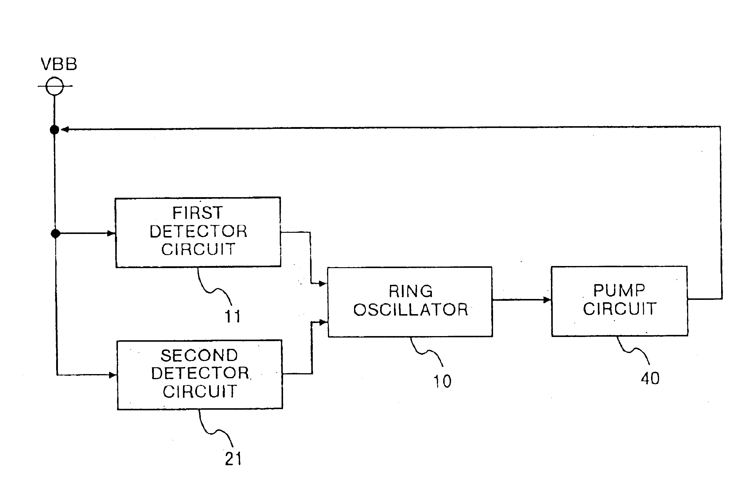
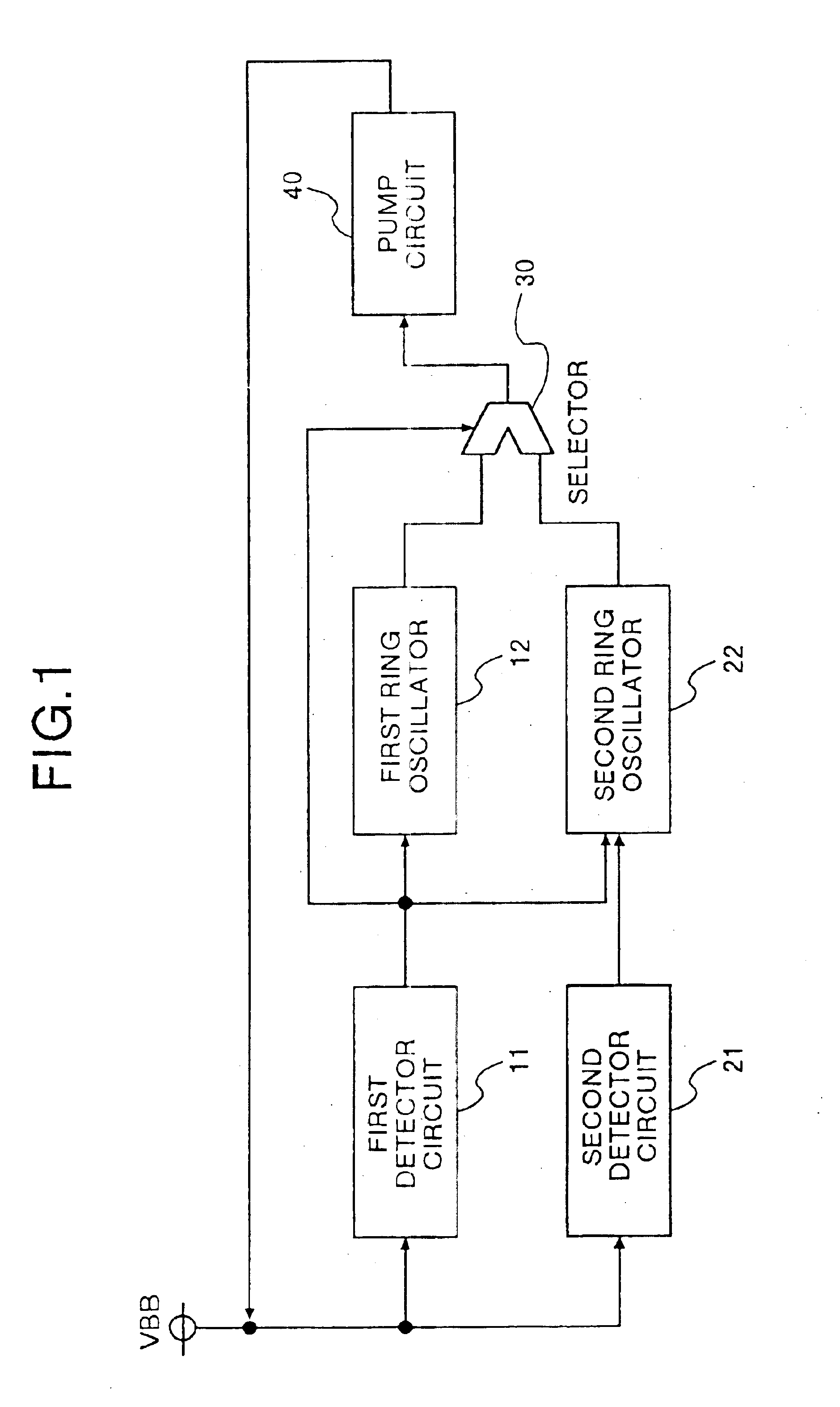
That is, the substrate bias voltage generating circuit of the first embodiment commonly uses one pump circuit 40, and determines the pumping voltage to be input to the pump circuit 40 in accordance with a value of the VBB voltage.
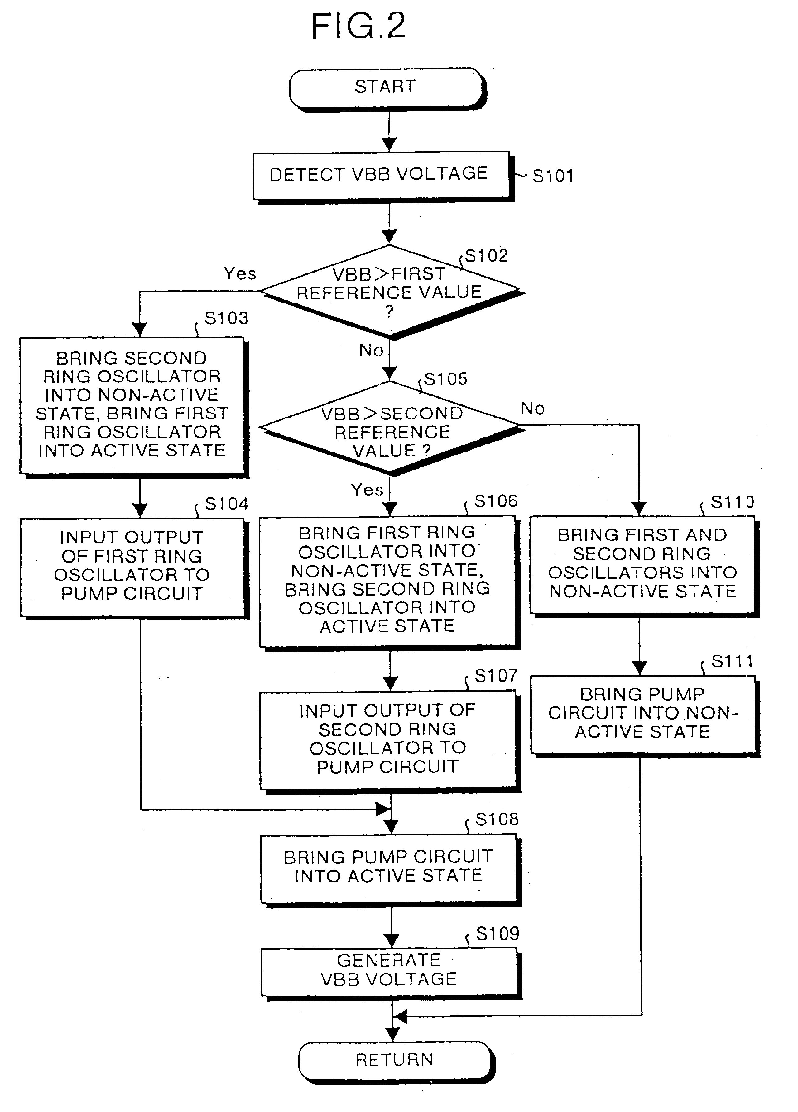
Next, the operation of the substrate bias voltage generating circuit of the first embodiment will be explained. FIG. 2 is a flowchart showing the operation of the substrate bias voltage generating circuit of the first embodiment. First, in the substrate bias voltage generating circuit, VBB voltage is input to the first detector circuit 11 and the second detector circuit 21 to detect the VBB voltage (step S101).
In the first detector circuit 11, if it is detected that the input VBB voltage is greater than the first reference value (e.g., -0.8V) (YES in step S102), the first detector circuit 11 outputs the first detector signal. This first detector signal is input to the first ring oscillator 12 to bring the latter into the active state (step S103). At that ti...
third embodiment
The substrate bias voltage generating circuit shown in FIG. 5 is different from that shown in FIG. 1 in that the former substrate bias voltage generating circuit has one ring oscillator, and a pumping voltage is tuned in accordance with the first and second detector signals in the ring oscillator 10. Thus, the third embodiment has a feature also in the inside structure of the ring oscillator 10.
FIG. 6 is a circuit diagram of a ring oscillator 10 of the substrate bias voltage generating circuit of the third embodiment. In FIG. 6, the ring oscillator 10 comprises an NOR gate G21 to which the first and second detector signals are input, inverters G22 and G23 for sequentially inverting an output of the NOR gate G21, and an NAND gate G24. An output from the inverter G23 is input to one of input terminals of the NAND gate G24.
The ring oscillator 10 further comprises an initial delay group comprising a plurality of serially connected inverters, a first delay group serially connected to the...
second embodiment
That is, when the first detector signal is output in the first detector circuit 11, a pumping voltage having a frequency determined by the delay of the m-number of inverters is generated, and when the second detector signal is output in the second detector circuit 21, a pumping voltage having frequency determined by the delay of the m+n number of inverters is generated. This means that the same effect as the second embodiment can be obtained.
Next, the operation of the substrate bias voltage generating circuit of the third embodiment will be explained. FIG. 7 is a flowchart showing the operation of the substrate bias voltage generating circuit of the third embodiment. First, in the substrate bias voltage generating circuit, VBB voltage is input to the first detector circuit 11 and the second detector circuit 21 to detect the VBB voltage (step S301)
In the first detector circuit 11, if it is detected that the input VBB voltage is greater than the first reference value (e.g., -0.8V) (YE...
PUM
 Abstract
Description
Claims
Application Information