
Methods and apparatus for diffractive optical processing using an actuatable structure

a technology of actuatable structure and diffractive optical processing, which is applied in the direction of multiplex communication, generator/motor, instruments, etc., can solve the problems of loss of efficiency, performance issues of conventional mems diffractive optical processors, and a variety of shortcomings of conventional spatial light modulators

Inactive Publication Date: 2004-04-20
MASSACHUSETTS INST OF TECH
View PDF93 Cites 12 Cited by
  • Summary
  • Abstract
  • Description
  • Claims
  • Application Information

AI Technical Summary

Benefits of technology

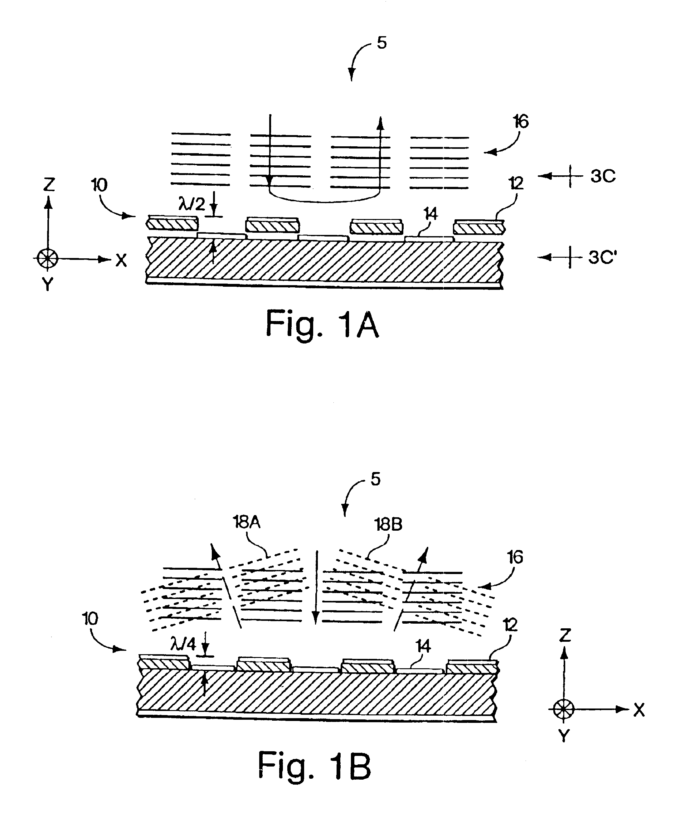
The present invention relates to optical processing using MEMS technology. More specifically, it focuses on improving the control of actuation in grating elements to achieve better optical processing functions. The invention proposes the use of a support structure to hold the grating elements in place, allowing for better control of separation between them. This results in more efficient and controlled diffraction of light, leading to improved performance and functionality in optical communication systems. The invention also addresses the issue of speed of operation, range of actuation, and physical size of the spatial light modulator. Overall, the invention provides better control over optical processing functions using MEMS technology.

Problems solved by technology

As a result, conventional MEMS diffractive optical processors have performance issues related to the loss of efficiency arising from the inability to adequately control the MEMS grating structure.
Some additional performance issues relevant to MEMS structures are speed of operation, range of actuation, and physical size of the spatial light modulator.
Conventional spatial light modulators suffer from a variety of shortcomings in connection with at least some of the above performance issues.

Method used


Image

  • Methods and apparatus for diffractive optical processing using an actuatable structure
  • Methods and apparatus for diffractive optical processing using an actuatable structure
  • Methods and apparatus for diffractive optical processing using an actuatable structure

Examples


Embodiment Construction

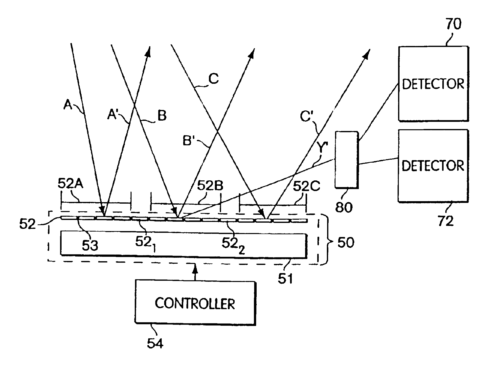
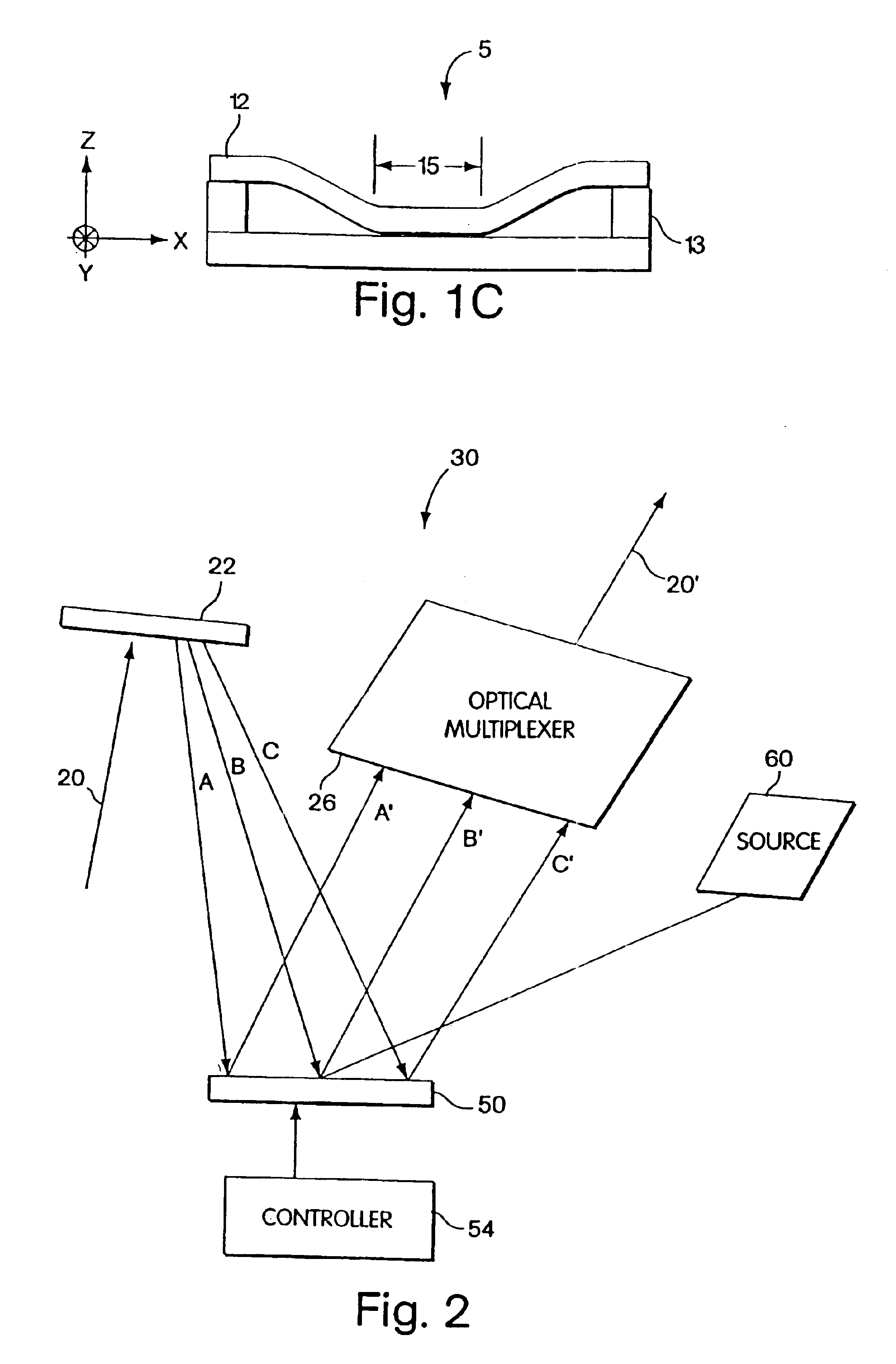
FIG. 2 is a diagram of an optical processing apparatus 30 (also referred to as an optical processor) illustrating aspects of the present invention. In FIG. 2, an optical signal 20 (e.g., from an input optical fiber (not shown) to the apparatus 30) having a number of optical carriers (i.e., signal 20 is a WDM signal) is directed to an optical demultiplexer 22. The optical demultiplexer 22 may include one or more optical elements to spatially separate different wavelengths of the optical signal 20. In one aspect of this embodiment, a fixed transmission or reflection diffraction grating may be employed as the optical demultiplexer 22 (e.g., FIG. 2 illustrates a reflective element for the optical demultiplexer), although it should be appreciated that the invention is not limited in this respect; namely, other types of conventional optical elements may be used for the optical demultiplexer 22.

In one aspect of the invention, the purpose of the demultiplexer 22 is to achieve spatial separa...


PUM


Abstract

A method of redirecting light using an actuatable two-layer diffraction grating structure, the method having applications in wavelength-division multiplexed systems. An optical add / drop modulator (OADM) including an actuatable diffraction grating, for use with a wavelength-division multiplexed signal. An OADM having an optical source located off the main pathway to direct a optical carrier to be added onto the actuatable diffraction grating such that the carrier is diffracted into the main pathway. A detector to measure signal strength for use with an optical processor, the optical processor having an actuatable structure having gaps between the actuated portion of the structure. The detector detecting the portions of light diffracted by the gaps.

Description

The present invention generally relates to optical processing using an actuatable structure and, more particularly, to methods and apparatus that facilitate a variety of optical processing functions using a diffractive actuatable optical processor.DISCUSSION OF THE RELATED ARTMicroelectromechanical systems (MEMS) are being employed in an increasing range of applications. The desirability of employing MEMS arises in part because of the ability to batch fabricate such microscale systems with a variety of highly complex features and functionality. Optical processing is one area where MEMS have been used in an increasing number of applications. In particular, MEMS have been used to modulate the intensity of light.One method of achieving optical modulation using MEMS is by diffractive optical processing. As is conventionally known, the process of diffraction refers to a change in direction and / or intensity of radiation of a given wavelength after the radiation impinges upon a diffracting...

Claims


Application Information

Patent Timeline
Patent Type & Authority Patents(United States)
IPC IPC(8): B81B3/00G02B26/08G02B6/34H02N1/00G02B6/35H04J14/02
CPCG02B6/2931G02B6/29383G02B6/3516G02B6/357G02B6/3588G02B6/4246G02B26/0808H02N1/006H04J14/0201G02B6/3524G02B6/356G02B6/3584G02B6/3594G02B6/3598H04J14/0204H04J14/0205H04J14/0213
Inventor HUNG, ELMER S.DEUTSCH, ERIK R.SENTURIA, STEPHEN D.
Owner MASSACHUSETTS INST OF TECH
Learn More