Multi-layer structure and method for forming a thermal interface with low contact resistance between a microelectronic component package and heat sink

a microelectronic component and heat sink technology, applied in the direction of chemistry apparatus and processes, synthetic resin layered products, coatings, etc., can solve the problems of changing the performance characteristics of the component and/or destroying the component, excessive pressure can create detrimental and undesirable stresses, and the gap between the surfaces of the microelectronic component may be relatively wide and irregular

Inactive Publication Date: 2004-07-13
THERMAGON
View PDF5 Cites 39 Cited by
  • Summary
  • Abstract
  • Description
  • Claims
  • Application Information

AI Technical Summary

Problems solved by technology

Exceeding these limits can change the performance characteristics of the component and / or damage the component.
However, excessive pressure can create detrimental and undesirable stresses.
Since the microelectronic package and heat sink do not generally have smooth and planar surfaces a relatively wide and irregular gap may form between the surfaces of the microelectronic component and heat sink.
The use of thermal grease, paste or phase change materials cannot presently accommodate large variations in gap sizes.
Higher thermal resistance equates to poorer performance and is unacceptable.
In fact a thin layer of low melting metallic alloy cannot be swaged to a sheet of untreated copper or aluminum foil even at very high pressures without causing delamination.

Method used


Image

  • Multi-layer structure and method for forming a thermal interface with low contact resistance between a microelectronic component package and heat sink
  • Multi-layer structure and method for forming a thermal interface with low contact resistance between a microelectronic component package and heat sink
  • Multi-layer structure and method for forming a thermal interface with low contact resistance between a microelectronic component package and heat sink

Examples


example 11

A multi-layer composite with a carrier layer material of copper and a layer of a low melting indium alloy on opposite sides thereof was tested with the thickness of the carrier layer varied as shown below in Table D:

The tests in the above table D were conducted to show that differences in thickness of the core material do not materially change the thermal resistance of the sandwich multi-layer structure. The thermal resistance is due more to the interface resistance between component and composite than to the inherent thermal resistance due to thickness changes in the core material. This is because copper has a thermal conductivity of about 300 W / mK, and therefore does not contribute significantly to the thermal resistance.

example 111

A similar test was conducted using aluminum as the core material with the results shown below in Table E:

The tests in the above table E clearly show that differences in thickness of the aluminum do not materially change the thermal resistance of the sandwich multi-layer structure even for drastic changes in aluminum thickness.

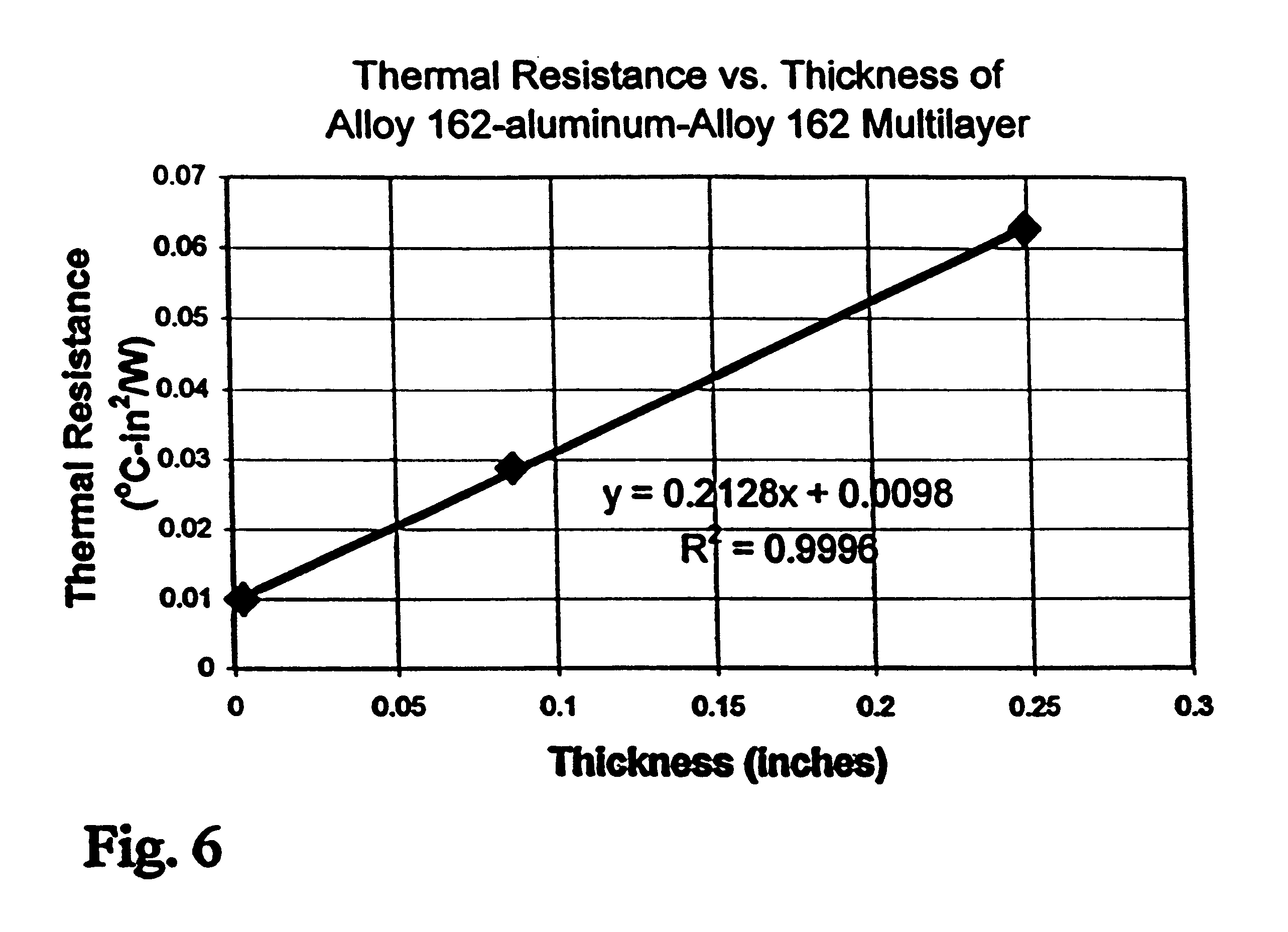
If the thermal resistance of the three composite samples are plotted against thickness (x axis) as shown in FIG. 6 the thermal conductivity can be calculated. The thermal conductivity is the inverse of the slope of the graph and may be calculated by the following equation:

Thermal conductivity=1 / slope

Thermal conductivity=1 / 0.2128.degree. C.in / W.multidot.39.4 in / m=185 W / mK

The measured thermal conductivity is reasonable for aluminum.

example 1v

Experiments were also run on a multi-layer structure as shown below in Table F to show that the surface finish of the platens would have little effect on the thermal performance of the sandwich structure. The exact surface finish of the roughened platens is not known but the gap with no interface material, referred to as "dry gap" was measured for the roughened surfaces to compare with the normal platens polished to a surface finish of 0.4 micrometers.

The above table F shows that the sandwich thermal resistance is not affected greatly by differences in surface finish and tolerance issues.


PUM

PropertyMeasurementUnit
thicknessaaaaaaaaaa
melting temperatureaaaaaaaaaa
pressureaaaaaaaaaa

Abstract

A multi-layer solid structure and method for forming a thermal interface between a microelectronic component package and a heat sink so that the structure has a total thermal resistance of no greater than about 0.03° C.-in<2>/W at a pressure of less than 100 psi. The structure comprises at least two metallic layers each of high thermal conductivity with one of the two layers having phase change properties for establishing low thermal resistance at the interface junction between the microelectronic component package and the heat sink.

Description

BACKGROUND OF THE INVENTIONMicroelectronic components, such as semiconductors, generate substantial heat which must be removed to maintain the component's junction temperature within safe operating limits. Exceeding these limits can change the performance characteristics of the component and / or damage the component. The heat removal process involves heat conduction through an interface material from the microelectronic component to a heat sink. The selection of the interface material and the thermal resistance at the interface between the heat generating component (e.g. silicon ic chip) and the heat sink controls the degree of heat transfer. As the demand for more powerful microelectronics increase so does the need for improved heat removal.The thermal resistance between the microelectronic component package and the heat sink is dependent not only upon the intrinsic thermal resistance of the interface material but also upon the contact interface thermal resistance formed at the junc...

Claims


Application Information

Patent Timeline
Patent Type & Authority Patents(United States)
IPC IPC(8): H01L23/427H01L23/34
CPCH01L23/4275H01L2924/3011Y10S165/907H01L2924/0002H01L2924/00
Inventor HILL, RICHARD F.HAMPTON, III, FOREST
Owner THERMAGON
Why Eureka
Try Eureka