FinFET-based SRAM cell

a sram cell and finfet technology, applied in the field of semiconductor devices and semiconductor manufacturing, can solve the problems of conventional mosfets that have difficulty scaling below 50 nm fabrication processing

Inactive Publication Date: 2004-07-20
GLOBALFOUNDRIES US INC
View PDF3 Cites 136 Cited by
  • Summary
  • Abstract
  • Description
  • Claims
  • Application Information

AI Technical Summary

Problems solved by technology

Conventional MOSFETs have difficulty scaling below 50 nm fabrication processing.

Method used


Image

  • FinFET-based SRAM cell
  • FinFET-based SRAM cell
  • FinFET-based SRAM cell

Examples


Embodiment Construction

refers to the accompanying drawings. The same reference numbers may be used in different drawings to identify the same or similar elements. Also, the following detailed description does not limit the invention. Instead, the scope of the invention is defined by the appended claims and equivalents.

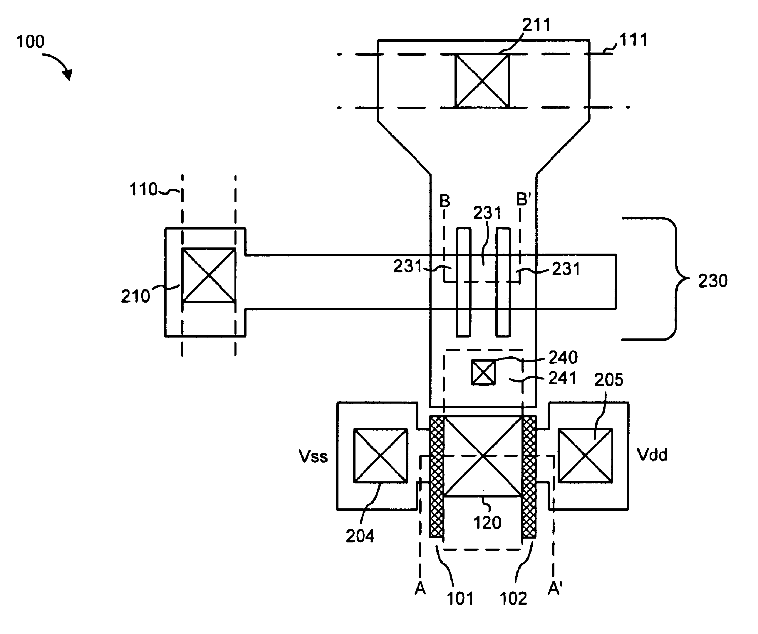
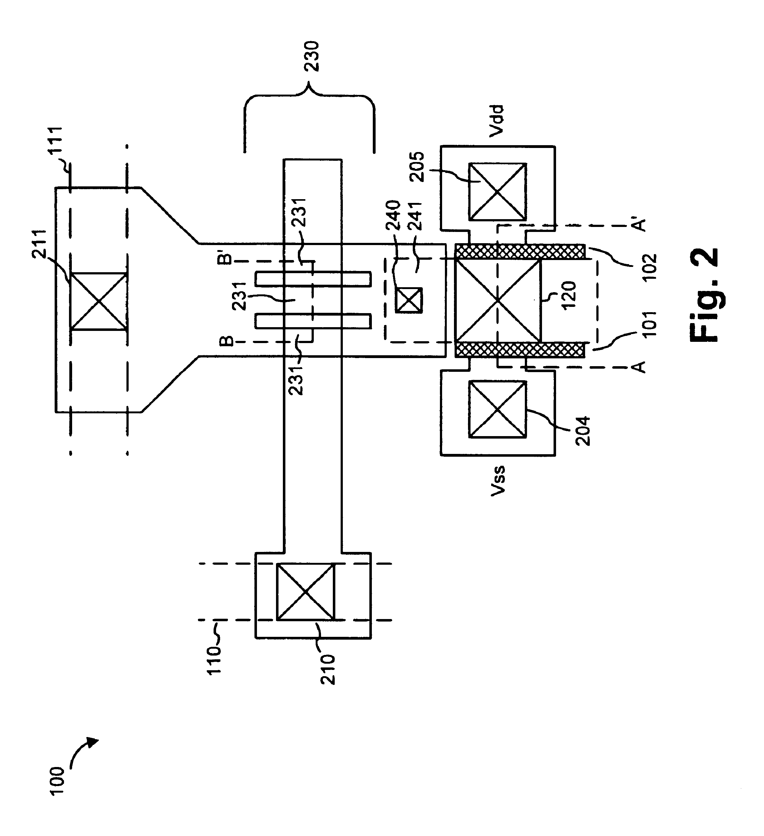
An SRAM cell includes a single FinFET and two tunnel diodes. The diodes may be formed using a FinFET-type fin structure. The FinFET may include multiple fins, which help to increase current through the pass gate and improve read time.

SRAM Cell

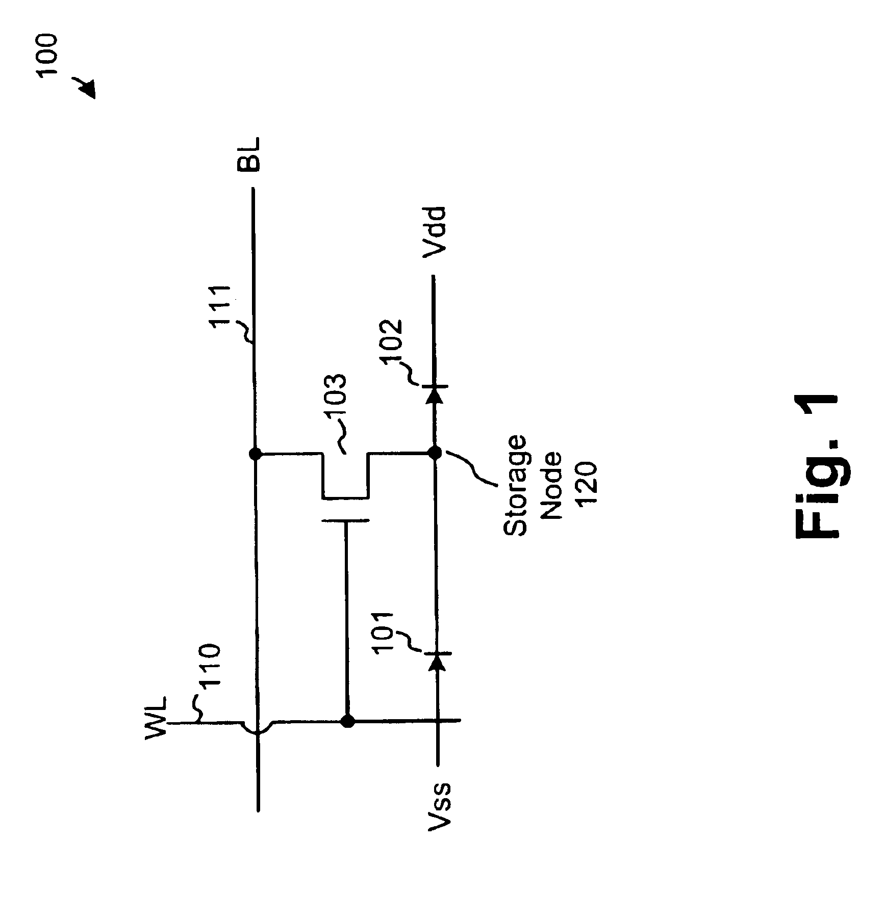
FIG. 1 is a schematic circuit diagram of an SRAM cell 100. Two tunnel diodes 101 and 102 are connected in series between a voltage source (Vss) and a voltage ground (Vdd). Word line (110) and bit line (111) control reading / writing to the SRAM cell 100. A switch 103, such as a MOSFET, is connected at its source to BL 111, at its gate to WL 110, and at its drain to node 120. Node 120 acts as the data storage node for the SRAM cell 100.

Tunnel diodes 101 an...


PUM


Abstract

A SRAM cell includes a single FinFET and two resonant tunnel diodes. The FinFet has multiple channel regions formed from separate fins. The resonant tunnel diodes may be formed from FinFET type fins. In particular, the resonant diodes may includes a thin, undoped silicon region surrounded by a dielectric. The SRAM cell is small and provides fast read/write access times.

Description

A. Field of the InventionThe present invention relates generally to semiconductor manufacturing and semiconductor devices and, more particularly, to static random access memories (SRAMs).B. Description of Related ArtSRAM is random access memory that retains its stored data as long as power is supplied to the SRAM cells. Unlike dynamic RAM (DRAM), which stores bits in cells consisting of a capacitor and a transistor, SRAM does not have to be periodically refreshed. SRAM generally provides faster memory bit access than DRAM.One conventional SRAM cell include six transistors arranged as cross-coupled inverters to form a flip-flop. Other conventional SRAM cells include a single transistor and two tunnel diodes. The single transistor in this SRAM may be a MOSFET type transistor.Conventional MOSFETs have difficulty scaling below 50 nm fabrication processing. To develop sub-50 nm MOSFETs, double-gate MOSFETs have been proposed. In several respects, the double-gate MOSFETs offer better char...

Claims


Application Information

Patent Timeline
Patent Type & Authority Patents(United States)
IPC IPC(8): H01L21/70H01L27/11H01L21/8244G11C11/412
CPCB82Y10/00G11C11/412H01L27/11H01L29/66818H01L29/785Y10S257/903H10B10/00
Inventor KRIVOKAPIC, ZORANAN, JUDY XILINBUYNOSKI, MATTHEW S.
Owner GLOBALFOUNDRIES US INC
Why Eureka
Try Eureka