

Imaging optical system and exposure apparatus
an optical system and exposure apparatus technology, applied in the direction of photomechanical apparatus, instruments, printers, etc., can solve the problems of difficult illumination system design, no na on the order, and difficult beam isolation
- Summary
- Abstract
- Description
- Claims
- Application Information
AI Technical Summary
Benefits of technology
Problems solved by technology
Method used
Image

Examples
Embodiment Construction
1. Field of the Invention
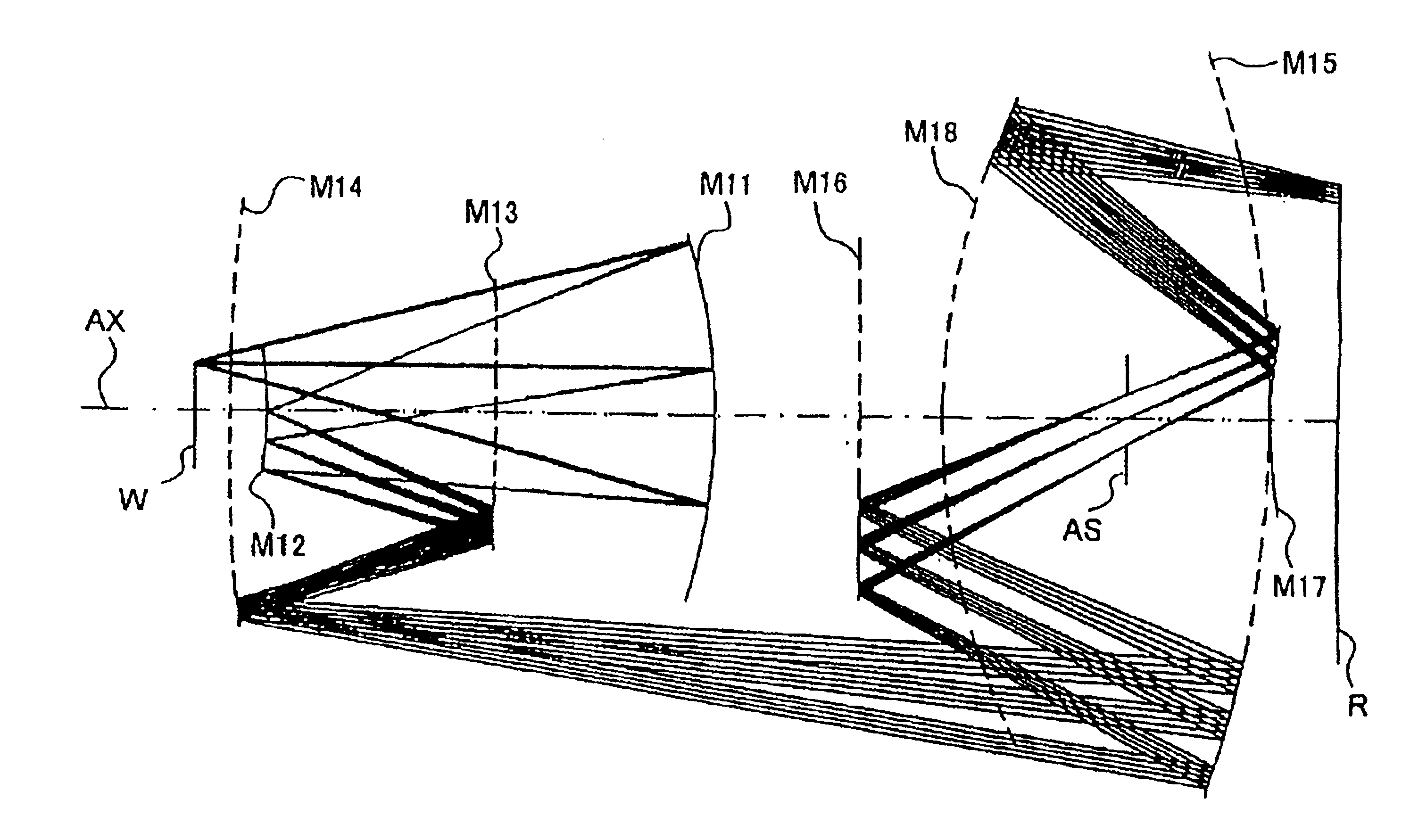
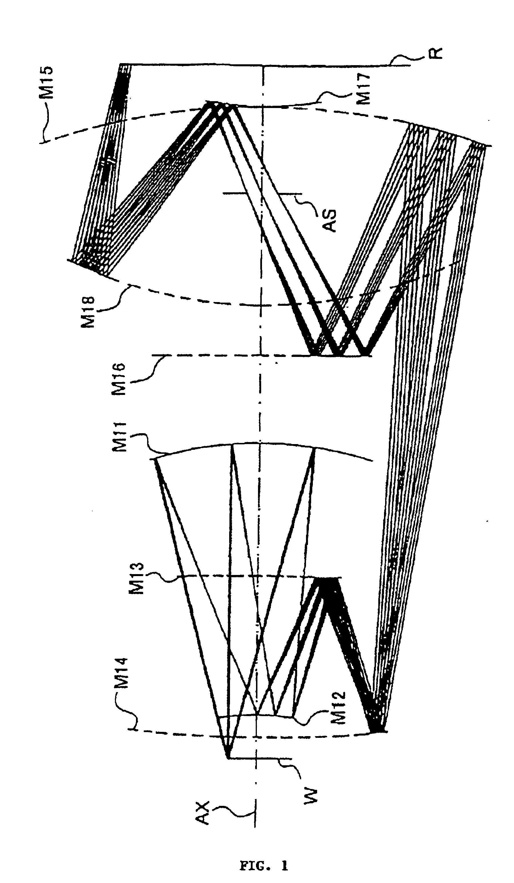
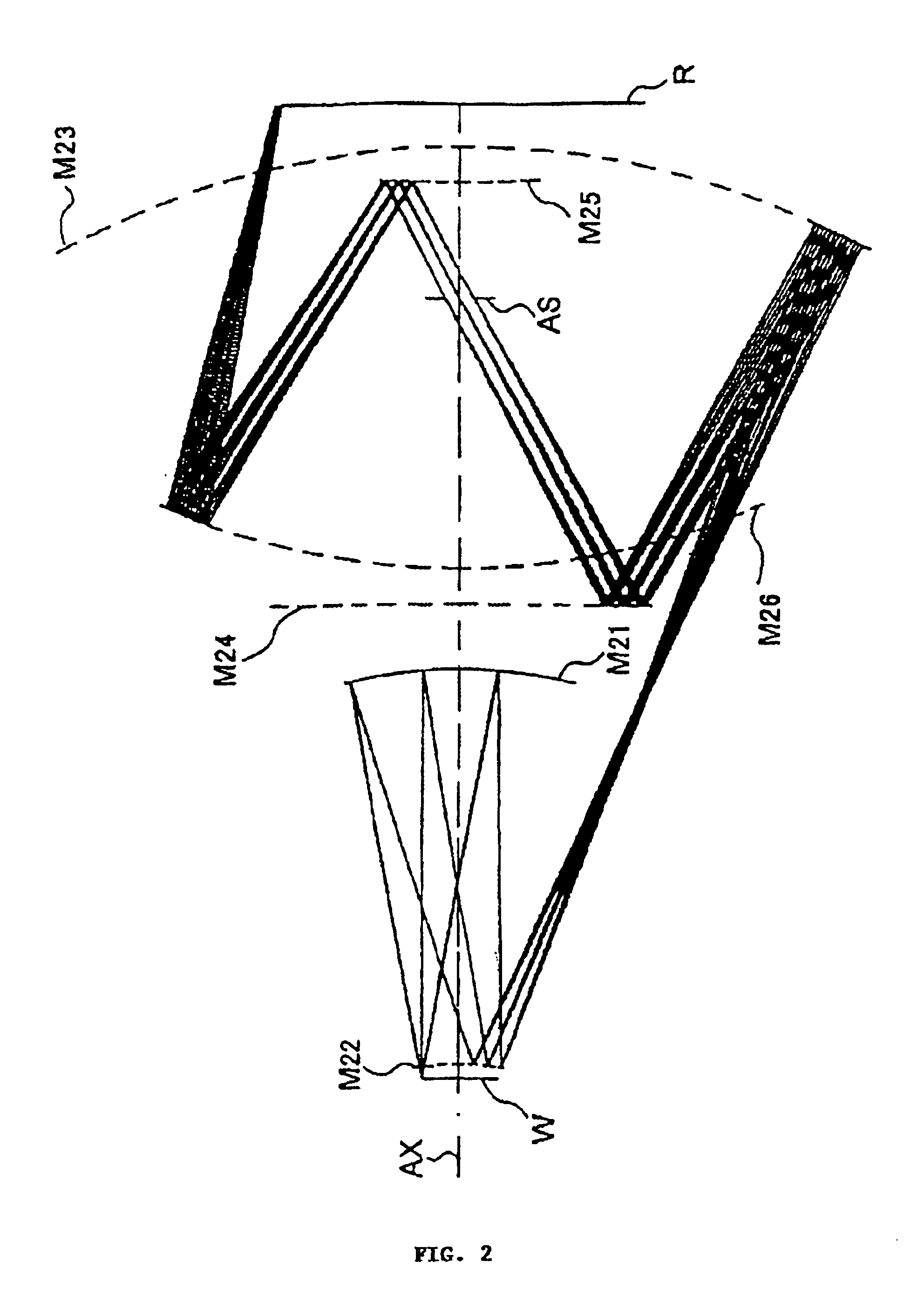
The present invention pertains to an imaging optical system and exposure apparatus which may be favorably used during manufacture for example of semiconductor elements, liquid crystal display elements, image pickup elements, CCD elements, thin-film magnetic heads, and / or other such microdevices through use of photolithographic techniques.
2. Background of the Invention
Minimum linewidths in circuit patterns grow smaller with each successive generation of technology in the semiconductor and like fields of art. With each such generation of technology, greater resolving power has therefore been demanded of the exposure apparatuses used in such fields of art, and the light used for exposure (hereinafter "actinic light") has moved to shorter and shorter wavelengths. Note that except where otherwise specified, "light" and "radiation" are used interchangeably herein and without intention to limit either to wavelengths which are visible or invisible or the like, both ...
PUM
| Property | Measurement | Unit |
|---|---|---|
| wavelength | aaaaa | aaaaa |
| wavelengths | aaaaa | aaaaa |
| wavelength | aaaaa | aaaaa |
Abstract
Description
Claims
Application Information