Chemical amplification type photoresist composition, method for producing a semiconductor device using the composition, and semiconductor substrate

a technology of photoresist and composition, which is applied in the direction of photomechanical equipment, instruments, photosensitive material processing, etc., can solve the problems of resist pattern resolution defects in the inside of the via-hole or its vicinity, deactivation of acid catalyst in the photoresist and hence shortage, and severe

Inactive Publication Date: 2004-10-05
SHIN ETSU CHEM CO LTD +1
View PDF11 Cites 25 Cited by
  • Summary
  • Abstract
  • Description
  • Claims
  • Application Information

AI Technical Summary

Benefits of technology

The photoresist, thus left, overlies the rim of the via-hole on the surface of the cap film 3, such that, when the wiring groove 22 is to be etched, the residual photoresist operates as a visor on the cap film 3, with the result that a protrusion 10 in the form of a tapered cylinder comprised of the cap film 3 and the second inter-layer insulating film 4 is formed around the outer rim of the via-hole (see FIG. 9g). If the low dielectric constant film (Low-k film) is used as the inter-layer insulating film, the protrusion 10 is increased in size. If the Cu dual Damascene wiring 9 is formed as the protrusion 10 is left over, separation or connection defects occur intermediate the wiring and the via-hole in the dual Damascene wiring 9, due to the protrusion 10, with the result that the electrical connection between the wiring and the via-hole in the dual Damascene wiring 9 is insufficient (see FIG. 9h). The result is the lowered reliability of the semiconductor device.
It is a third object of the present invention to provide a method for producing a semiconductor device which lends itself to simplification and speedup of the manufacturing process.

Problems solved by technology

According to the technical information, acquired by the present inventors, the reason this problem arises is that, if the anti-reflection film and the chemical amplification type photoresist composition are coated and exposed to light without pre-treatment (such as heating, UV processing or oxygen plasma processing), the pollutants, such as basic compounds or moisture, affixed to or soaked into the substrate surface (such as via-hole wall surface of the inter-layer insulating film), tend to be transmitted through the anti-reflection film at the time of baking the anti-reflection film and the photoresist (pre-baking for solvent removal) so as to be intruded into the photoresist.
Should this neutralization reaction between the pollutants and the acid catalyst occur, the acid catalyst in the photoresist is deactivated and hence falls into shortage.
As a consequence, resolution defects of the resist pattern occur in the inside of the via-hole or its vicinity.
An experiment conducted by the present inventors revealed that, although a satisfactory resist pattern could be resolved with the conventional chemical amplification type photoresist, in the absence of the via-hole, in case development was carried out for 30 minutes under the condition in which the poisoning occurs, the poisoning occurs severely around the via-hole, such that the resist pattern suffers from resolution deficiency.
Although the resistance against the poisoning can be improved by extending the development time duration to 60 seconds, the resolution was still insufficient.

Method used


Image

  • Chemical amplification type photoresist composition, method for producing a semiconductor device using the composition, and semiconductor substrate
  • Chemical amplification type photoresist composition, method for producing a semiconductor device using the composition, and semiconductor substrate
  • Chemical amplification type photoresist composition, method for producing a semiconductor device using the composition, and semiconductor substrate

Examples


Embodiment Construction

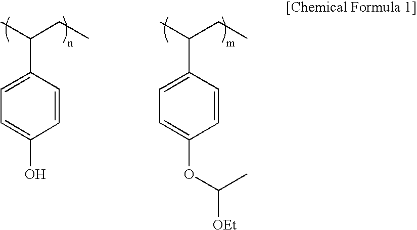
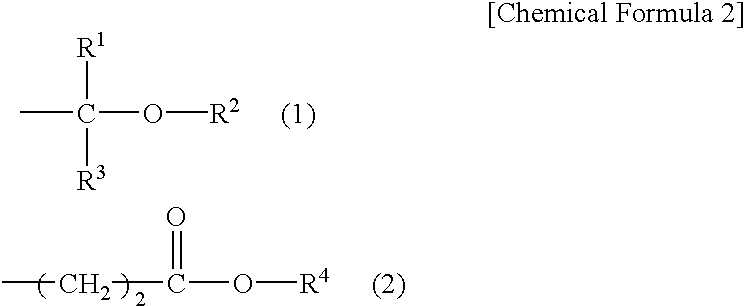
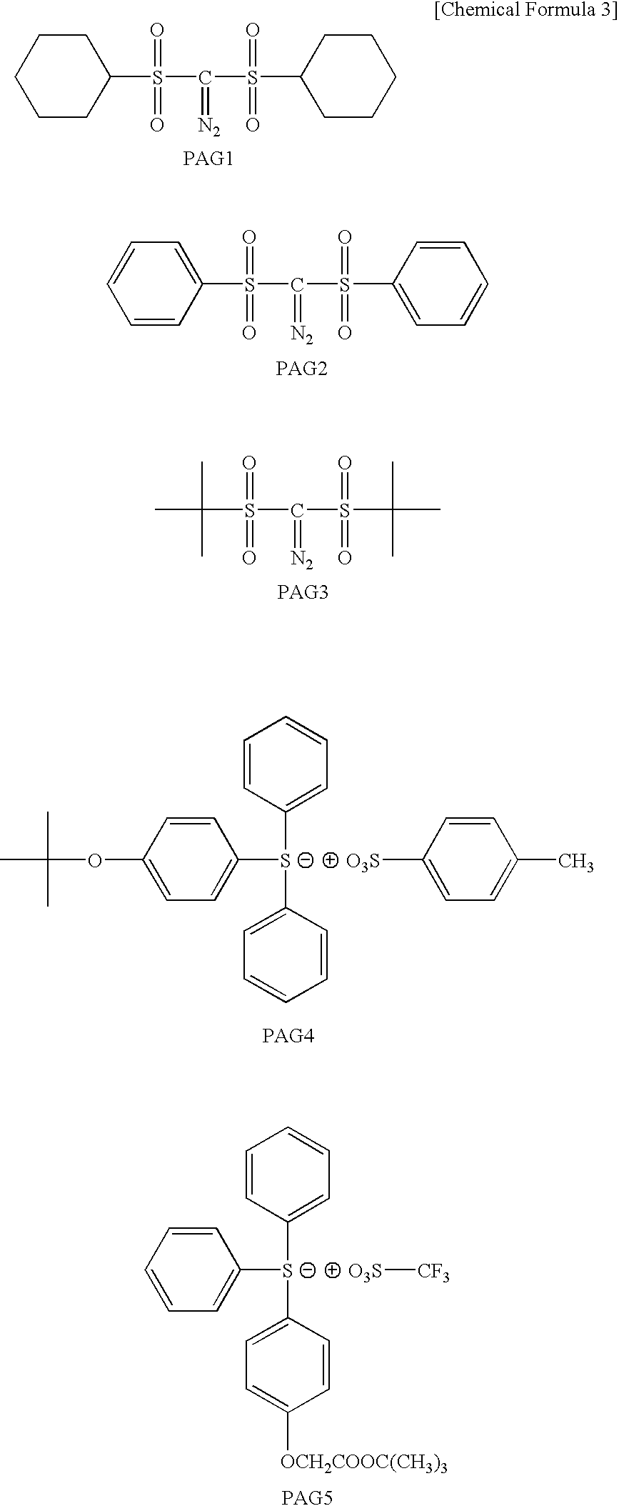
In the method for producing the semiconductor device, a resist film (1 of FIG. 1a) is formed on a substrate (semiconductor substrate) having a surface step difference (21 of FIG. 1a), using a chemical amplification type photoresist composition comprised of a base resin and a basic compound added to the base resin in a range of not less than 1 mmol to not more than 100 mmol to 100 g of the base resin, to form a resist film (1 of FIG. 1c), and a predetermined area of the resist film is exposed to light to form a resist pattern (1 of FIG. 1d). Even if the photoresist is poisoned by the poisoning component in the organic removing solution deposited to the vicinity of the step difference portion, it is possible to prevent the concentration of the acid catalyst from being lowered drastically, thanks to the buffering action of the basic compound in the resist. Thus, the light exposed portion of the resist can be converted into a substance soluble in the developing solution if the photoresi...


PUM

PropertyMeasurementUnit
dielectric constantaaaaaaaaaa
specific dielectric constantaaaaaaaaaa
dielectric constantaaaaaaaaaa

Abstract

To provide a chemical amplification type positive photoresist composition suited to resist patterning of a substrate presenting surface step differences, a method for manufacturing the semiconductor device employing this composition, and a semiconductor substrate. In a method for manufacturing a semiconductor device, a resist film is formed using a chemical amplification type positive photoresist composition, comprised of a base resin and a basic compound added to the base resin at a rate of 1 to 100 mmol to 100 g of the base resin, on a substrate halving surface step differences and into which the organic removing solution is deposited or oozed, and a predetermined area of the resist film is exposed to light to form a resist pattern.

Description

This invention relates to a chemical amplification (or chemically amplified) type [Kagakuzofuku-gata] photoresist composition, a method for producing a semiconductor device using the composition, and a semiconductor substrate. More particularly, it relates to a chemical amplification type photoresist composition for prohibiting resist pattern resolution defects, a method for producing a semiconductor device using the composition, and a semiconductor substrate.Definition: The term "chemical amplification (or chemically amplified) type photoresist" used herein denotes a class of the photoresist that falls within the following category:Chemical amplification type photoresist composition means a composition containing an acid generating agent as a sensitizer in the resist, generating acid therefrom upon light exposure, thus inducing the catalytic reaction by the generated acid during the subsequent heat treatment, thereby accelerating soluble or insoluble property against the developing...

Claims


Application Information

Patent Timeline
Patent Type & Authority Patents(United States)
IPC IPC(8): G03F7/004G03F7/039H01L21/02H01L21/70H01L21/027H01L21/768H01L21/312G03F7/38
CPCG03F7/0045G03F7/0392H01L21/0274H01L21/312H01L21/76828H01L21/76808Y10S438/949H01L21/76814H01L2221/1036H01L21/02203
Inventor NAGAHARA, SEIJISAKURADA, TOYOHISAYOSHIHARA, TAKAO
Owner SHIN ETSU CHEM CO LTD
Why Eureka
Try Eureka