Nano optical sensors via molecular self-assembly

a technology of optical sensors and molecular self-assembly, applied in the field of optical sensors, can solve the problems of reversible or tunable, once affecting the electronic properties of silicon,

Inactive Publication Date: 2004-11-09
HEWLETT-PACKARD ENTERPRISE DEV LP
View PDF3 Cites 47 Cited by
  • Summary
  • Abstract
  • Description
  • Claims
  • Application Information

AI Technical Summary

Benefits of technology

The present teachings offer a molecule-silicon hybrid electronic system, and utilize organic or organo-metallic molecules to modulate the semiconductor electronic properties in the nano regime, which could potentially produce optical sensing devices with much higher density and sensitivity.

Problems solved by technology

However, the molecules they discussed can only alter the silicon electronic properties once, not in a reversible or tunable fashion.

Method used


Image

  • Nano optical sensors via molecular self-assembly
  • Nano optical sensors via molecular self-assembly
  • Nano optical sensors via molecular self-assembly

Examples


Embodiment Construction

Reference is made now in detail to specific embodiments, which illustrates the best mode presently contemplated by the inventors for practicing the invention. Alternative embodiments are also briefly described as applicable.

Definitions

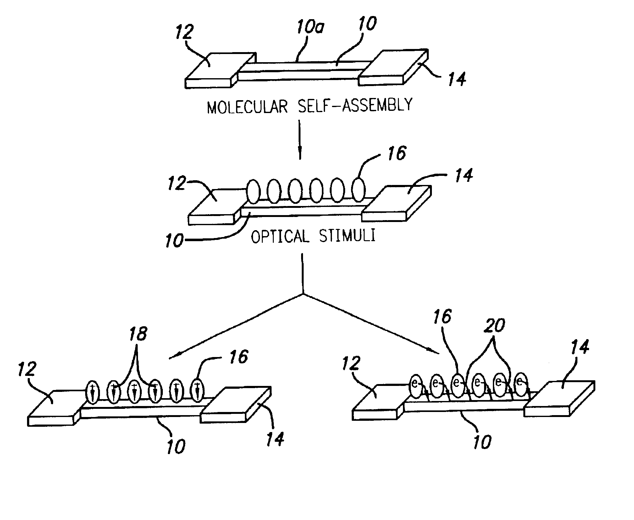
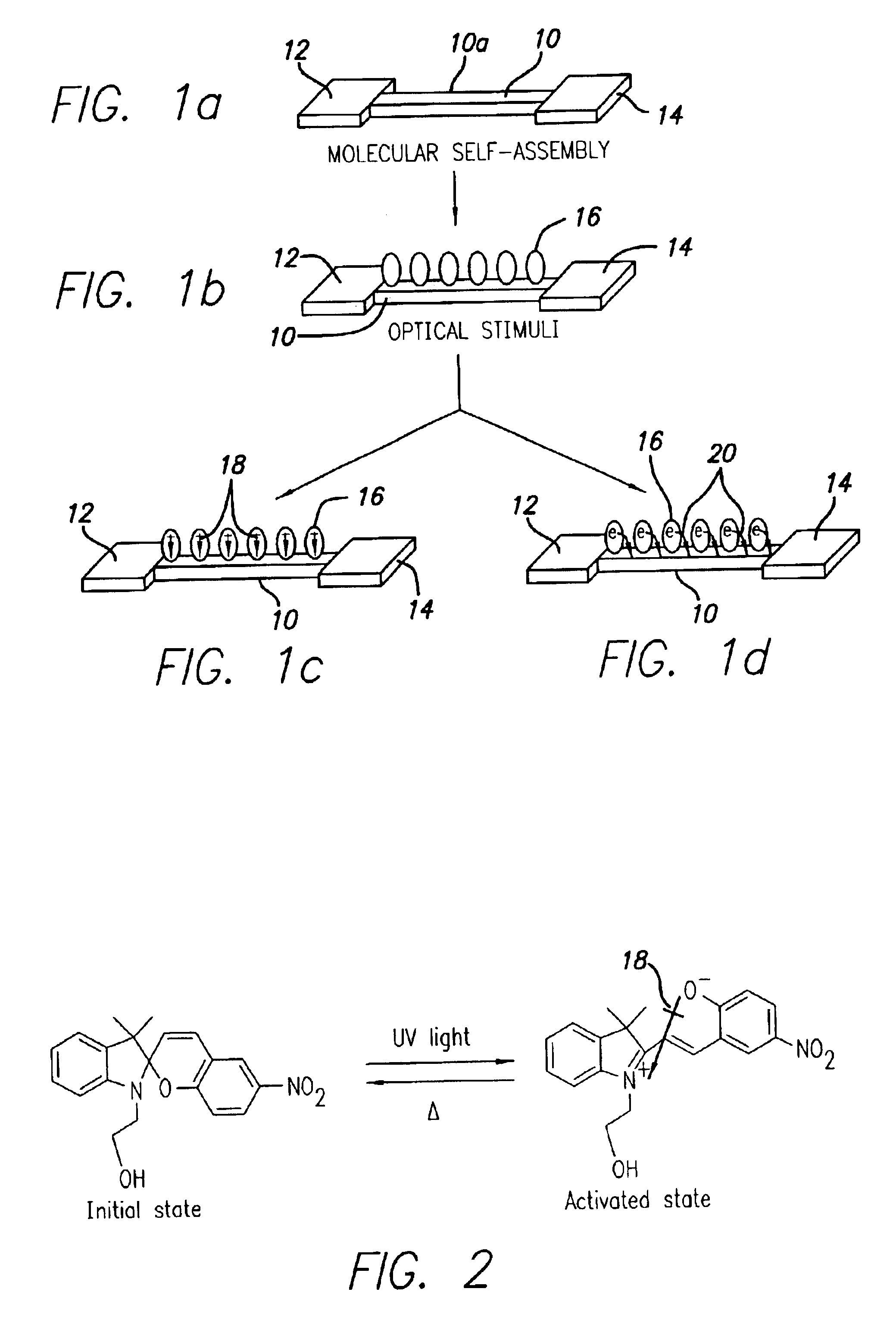
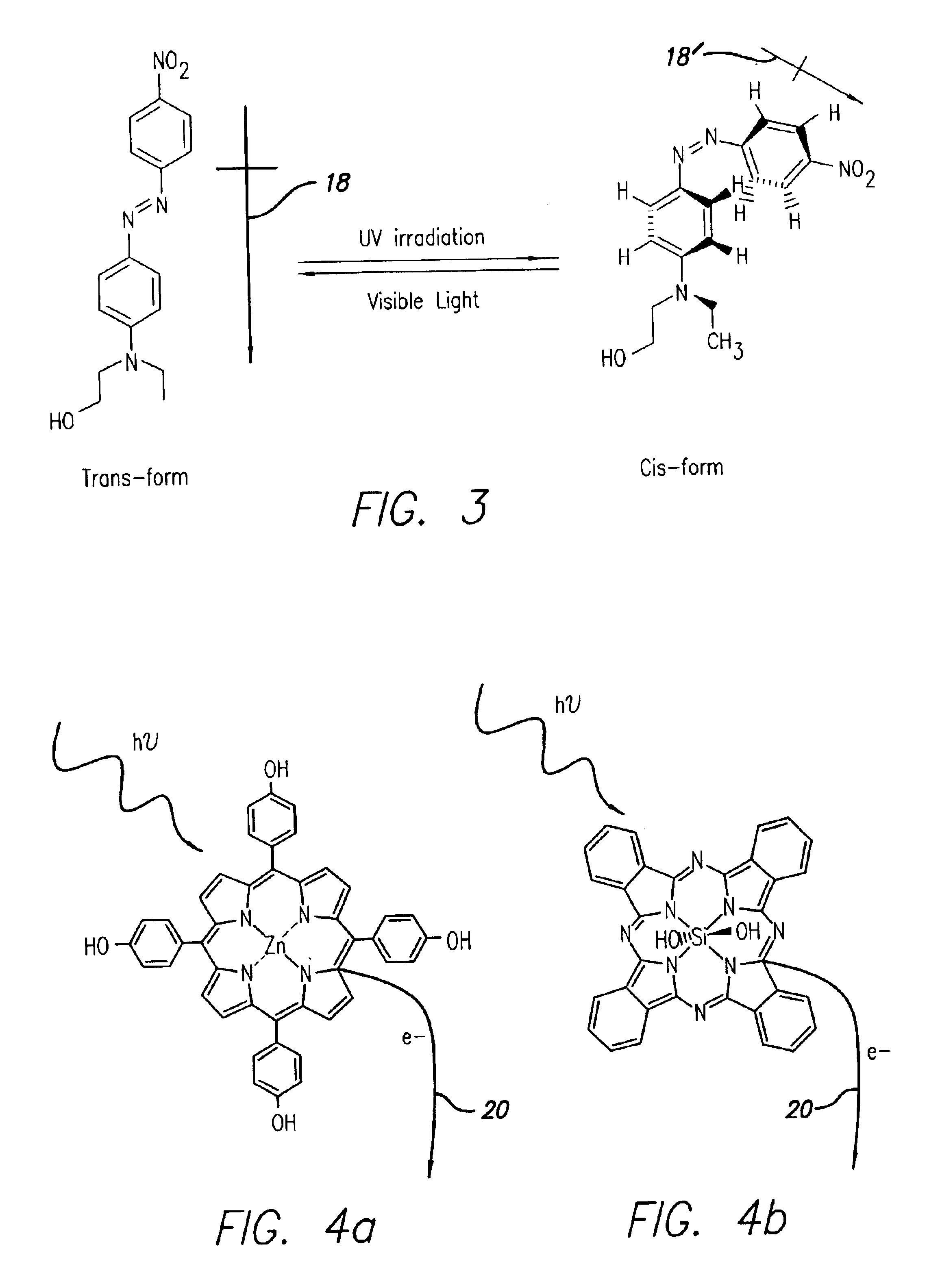
The term "self-assembled" as used herein refers to a system that naturally adopts some geometric pattern because of the identity of the components of the system; the system achieves at least a local minimum in its energy by adopting this configuration.

The term "singly configurable" means that a switch can change its state only once via an irreversible process such as an oxidation or reduction reaction; such a switch can be the basis of a programmable read-only memory (PROM), for example.

The term "reconfigurable" means that a switch can change its state multiple times via a reversible process such as an oxidation or reduction; in other words, the switch can be opened and closed multiple times, such as the memory bits in a random access memory (RAM) or a...


PUM


Abstract

An optical sensor is provided, comprising (a) a silicon nanowire of finite length having an electrical contact pad at each end thereof; and (b) a plurality of self-assembled molecules on a surface of the silicon nanowire, the molecules serving to modulate electrical conductivity of the silicon nanowire by either a reversible change in dipole moment of the molecules or by a reversible molecule-assisted electron / energy transfer from the molecules onto the silicon nanowire. Further, a method of making the optical sensor is provided. The concept of molecular self-assembly is applied in attaching functional molecules onto silicon nanowire surfaces, and the requirement of molecule modification (hydroxy group in molecules) is minimal from the point view of synthetic difficulty and compatibility. Self-assembly will produce well-ordered ultra-thin films with strong chemical bonding on a surface that cannot be easily achieved by other conventional methods.

Description

The present invention is directed to nano optical sensors and photodetectors, and, more particularly, to such devices and their fabrication, employing self-assembly of molecules which modulate the electrical conductivity in a silicon nanowire.Since the concept of molecular electronics was first proposed in 1974 by Aviram and Ratner (A. Aviram et al, Chemical Physics Letters, Vol. 29, pp. 277-283 (1974)), numerous studies have focused on probing single molecules in terms of using molecules directly as functional electric circuit components such as switches, diodes, or even transistors in replacement of conventional semiconductors, specifically, silicon. On another hand, the interaction of organic species with silicon surfaces remains a topic of considerable extent waiting to be explored, and the ability to tailor the surface electronic properties of silicon by organic or organo-metallic molecules poses a fascinating area hardly conceivable in the past. Cahen and coworkers (N. Zenou e...

Claims


Application Information

Patent Timeline
Patent Type & Authority Patents(United States)
IPC IPC(8): H01L51/05H01L51/30B82B1/00H01L29/22H01L31/0352H01L51/00
CPCH01L51/428H01L51/42H01L51/005H01L51/0071H01L51/0077Y02E10/549Y10S977/954H10K85/60H10K85/657H10K85/30H10K30/65H10K30/00
Inventor LI, ZHIYONGCHEN, YONGZHANG, SEAN XIAO-AN
Owner HEWLETT-PACKARD ENTERPRISE DEV LP
Why Eureka
Try Eureka