Hetero-structure photonic bandgap materials

a photonic bandgap and heterostructure technology, applied in the field of photonic bandgap materials, can solve the problems of single crystalline structure, unistructure, and inability to optimize the performance of a photonic integrated circuit (pic) in a single, and achieve the effects of improving throughput efficiency, back reflection, and reducing the size of the bandgap

Inactive Publication Date: 2004-12-14
UNIVERSITY OF DELAWARE
View PDF2 Cites 17 Cited by
  • Summary
  • Abstract
  • Description
  • Claims
  • Application Information

AI Technical Summary

Problems solved by technology

Optimizing the performance of a Photonic Integrated Circuit (PIC) in a single crystalline photonic crystal structure (unistructure) continues to be a challenge, due to the spatial constraint of the unistructure.
This limitation, namely single crystalline structures, has a pronounced impact over the bandgap size, throughput efficiency, and back reflections that arise due to spatial mismatches at transitions between different Photonic crystal sections such as straight and angular waveguides.
While this method can ensure an accurate solution for the dispersion properties of a photonic crystal structure, it is still limited due to the fact that transmission spectra, field distribution, and back reflections cannot be extracted, since it only considers propagating modes, whereas in a finite crystal there are also evanescent modes.
Presently, these operations have been hindered by the spatial constraints of the single crystalline structure, which in some cases limit their ability to efficiently perform their intended functions.
Such losses caused a mismatch between the waveguiding section 16 and the wavesplitting sections 18, 20, and hence reduced the overall throughput efficiency of the unistructure beam splitter.
In other words, due to geometrical limitations of the rectangular grid 12 on which the rectangular photonic crystal lattice was formed, unistructure beam splitter 10 did not achieve its predicted performance.
Even though other approaches were successfully capable of achieving better performance than the device 10 analyzed above, they still suffered from other issues such as waveguide directivity, that is, being a bi-directional waveguide instead of a unidirectional one.
Such techniques are better utilized for narrowband or selectively coupled devices, while their performance for broadband devices may not be optimal.

Method used


Image

  • Hetero-structure photonic bandgap materials
  • Hetero-structure photonic bandgap materials
  • Hetero-structure photonic bandgap materials

Examples


Embodiment Construction

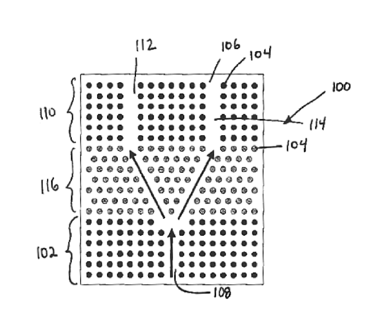
Reference will now be made in detail to the present preferred embodiment of the invention, an example of which is illustrated in the accompanying drawings. Wherever possible, the same reference numbers will be used throughout the drawings to refer to the same or like parts.

As used herein, the expression "optically communicates" refers to any connection, coupling, link or the like by which optical signals carried by one optical system element are imparted to the communicating element.

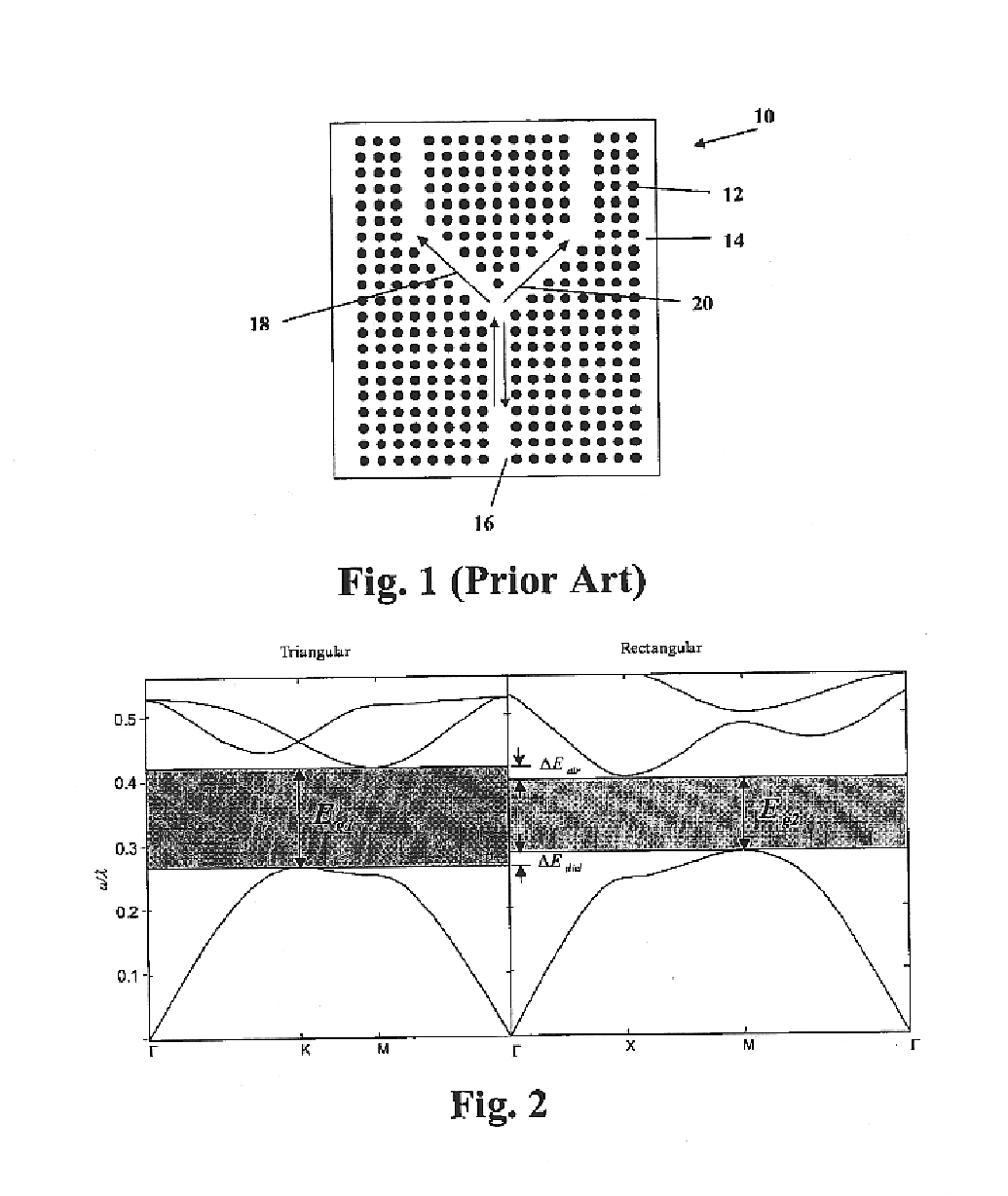
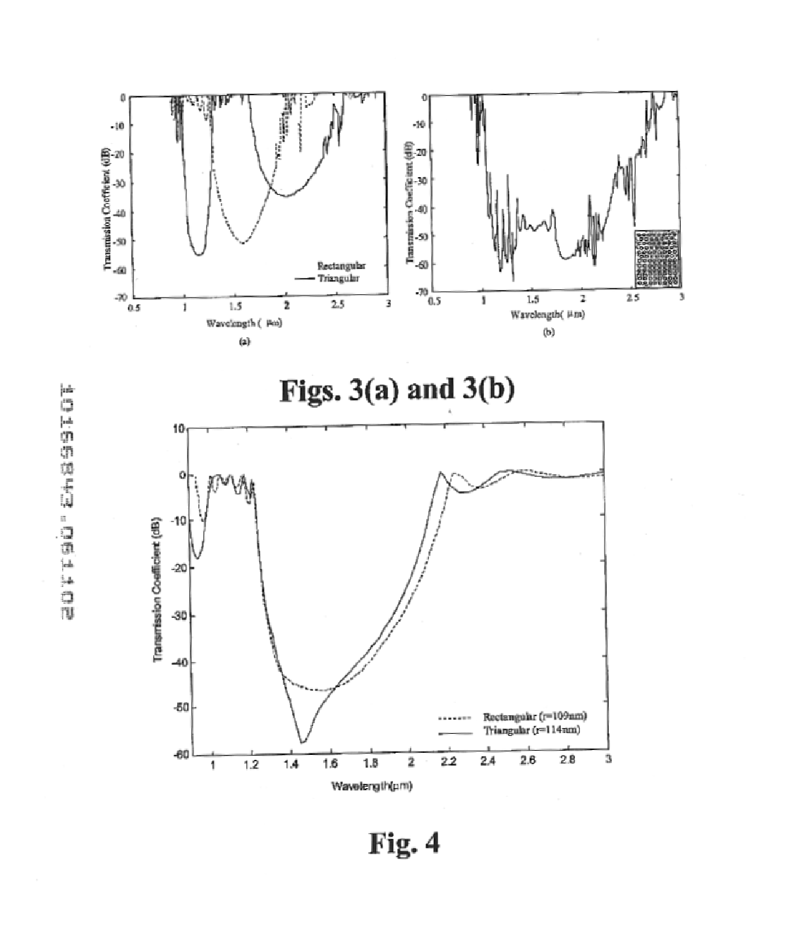
A. Localization of Light in Photonic Crystals

The physical phenomena that clearly describes the operation of a photonic crystal is the localization of light, which is achieved from the scattering and interference produced by a coherent wave in a periodic structure. In this case a photon located in a lossless dielectric media provides an ideal realization of a single excited state in a static medium at room temperature. To describe this phenomenon, Maxwell's equations are cast into a form similar to Schrod...


PUM


Abstract

A two-dimensional, hetero-structure photonic crystal includes a first rectangular lattice array of dielectric rods provided on a portion of an air background, and a second rectangular lattice array of dielectric rods provided on another portion of the air background. The two-dimensional, hetero-structure photonic crystal provides the advantages of both the rectangular and triangular lattice arrays for application with optical beam splitters and combiners, and achieves a transmission efficiency greater than 90% in comparison to the transmission efficiency of 50% for the conventional uni-structure photonic crystals.

Description

A. Field of the InventionThe present invention relates generally to photonic bandgap materials (also known as photonic crystals), and, more particularly to hetero-structure photonic bandgap materials.B. Description of the Related ArtDuring the last decade photonic crystals have risen from an obscure technology to a prominent field of research. In large part this is due to their unique ability to control, or redirect, the propagation of light. E. Yablonovich, "Inhibited spontaneous emission in solid-state physics and electronics," Physical Review Letters, vol. 58, pp. 2059-2062 (May 1987), and S. John, "Strong localization of photons in certain disordered dielectric superlattices," Physical Review Letters, vol. 58, pp. 2486-2489 (June 1987), initially proposed the idea that a periodic dielectric structure can possess the property of a bandgap for certain frequencies in the electromagnetic spectra, in much the same way as an electronic bandgap exists in semiconductor materials. This p...

Claims


Application Information

Patent Timeline
Patent Type & Authority Patents(United States)
IPC IPC(8): G02B6/125G02B6/122
CPCB82Y20/00G02B6/125G02B6/1225
Inventor PRATHER, DENNIS W.SHARKAWY, AHMED SAMIRSHI, SHOUYUN
Owner UNIVERSITY OF DELAWARE
Why Eureka
Try Eureka