Semiconductor substrate with defects reduced or removed and method of manufacturing the same, and semiconductor device capable of bidirectionally retaining breakdown voltage and method of manufacturing the same
- Summary
- Abstract
- Description
- Claims
- Application Information
AI Technical Summary
Benefits of technology
Problems solved by technology
Method used
Image

Examples
Embodiment Construction
="d_n">[0038]FIG. 28 is a graph showing a result of study on a relation between implantation depth of proton and the breakdown voltage;
[0039]FIG. 29 is a cross section showing a structure of a semiconductor device in accordance with a sixth preferred embodiment of the present invention, based on the semiconductor device shown in FIG. 24;
[0040]FIG. 30 is a cross section showing a structure of a semiconductor device in accordance with the sixth preferred embodiment of the present invention, based on the semiconductor device shown in FIG. 25;
[0041]FIG. 31 is a cross section showing a structure of a semiconductor device in accordance with a first variation of the sixth preferred embodiment of the present invention; and
[0042]FIG. 32 is a cross section showing a structure of a semiconductor device in accordance with a second variation of the sixth preferred embodiment of the present invention.
DESCRIPTION OF THE PREFERRED EMBODIMENTS
[0043]First Preferred Embodiment
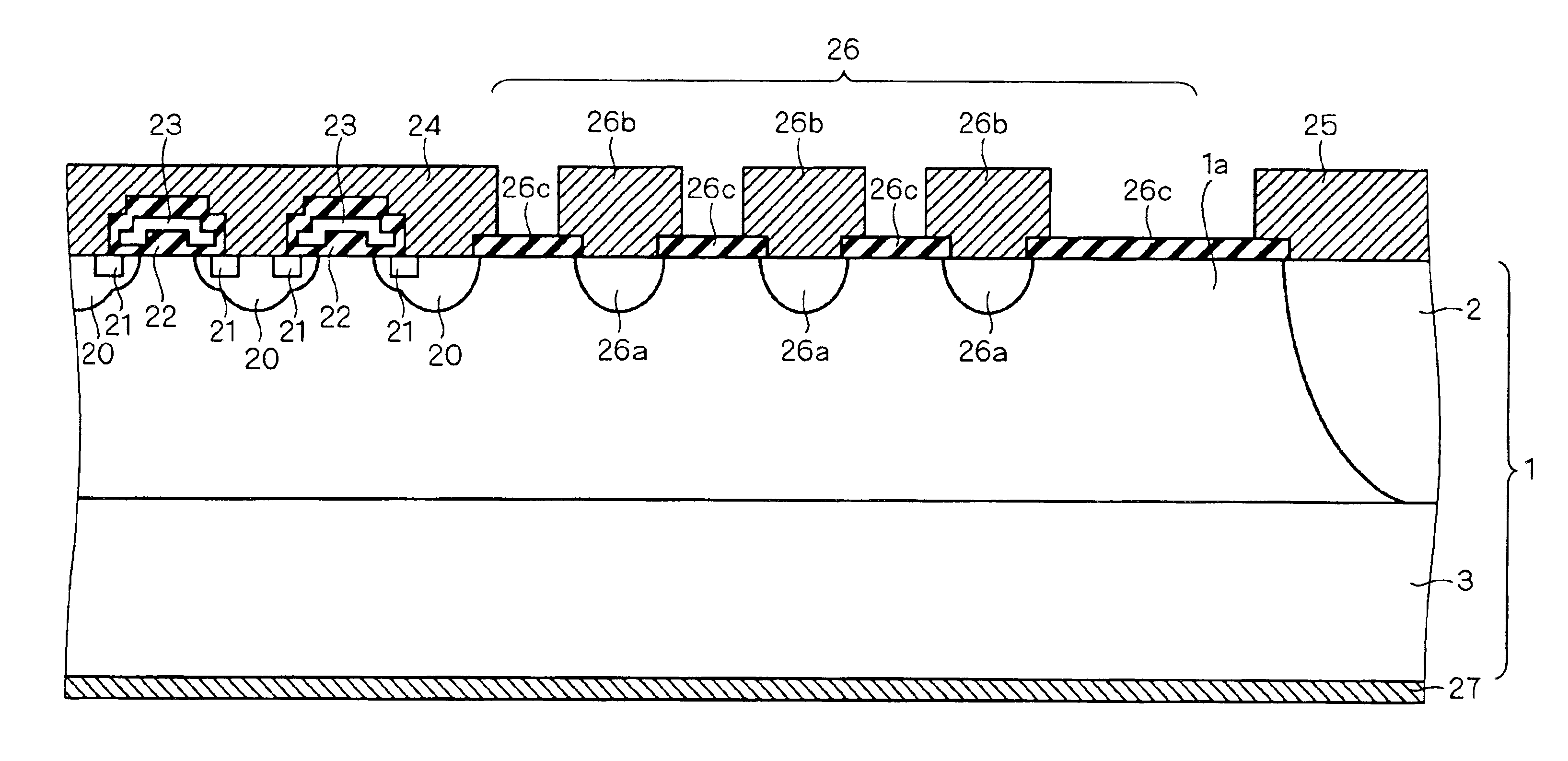
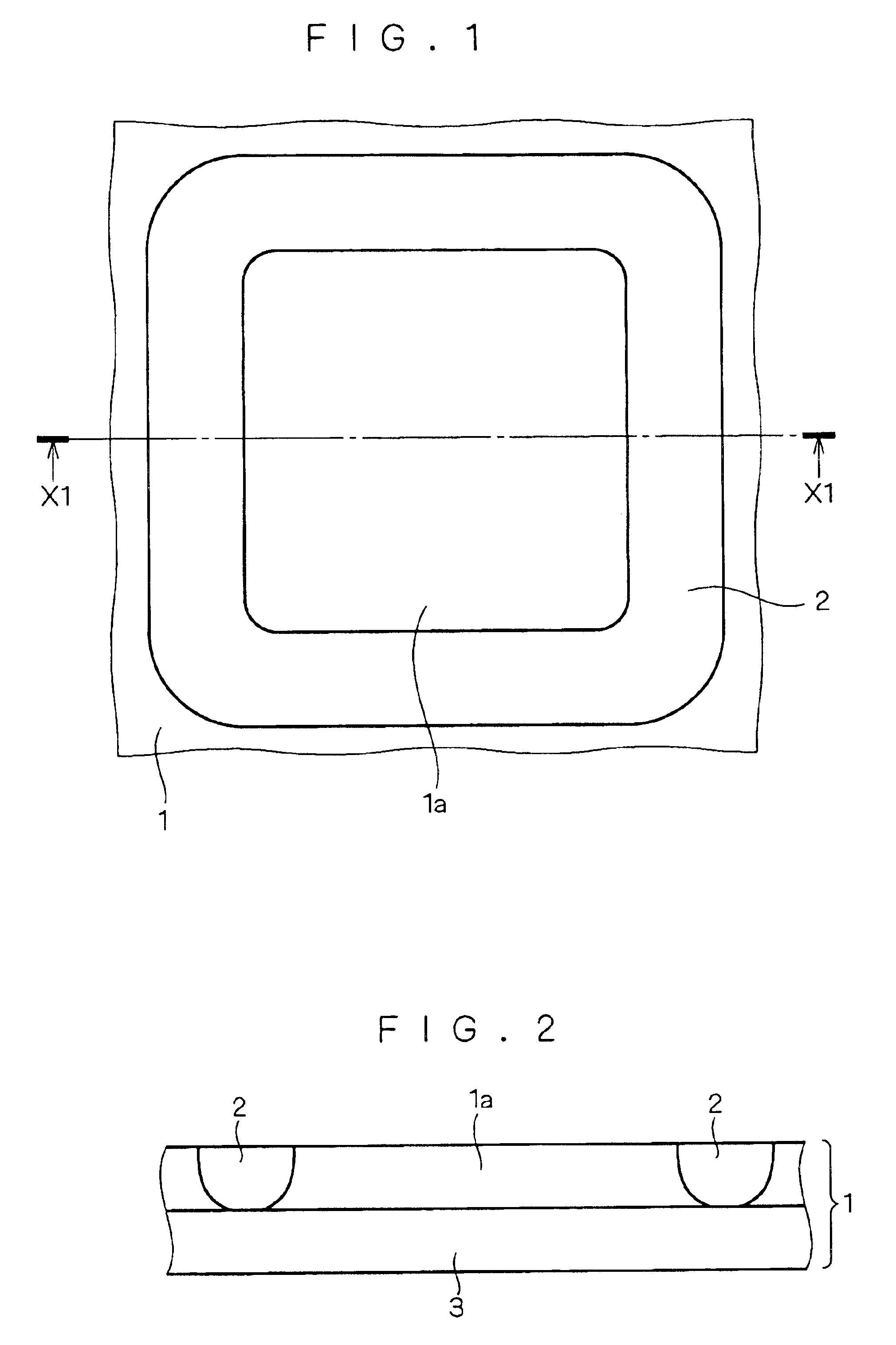
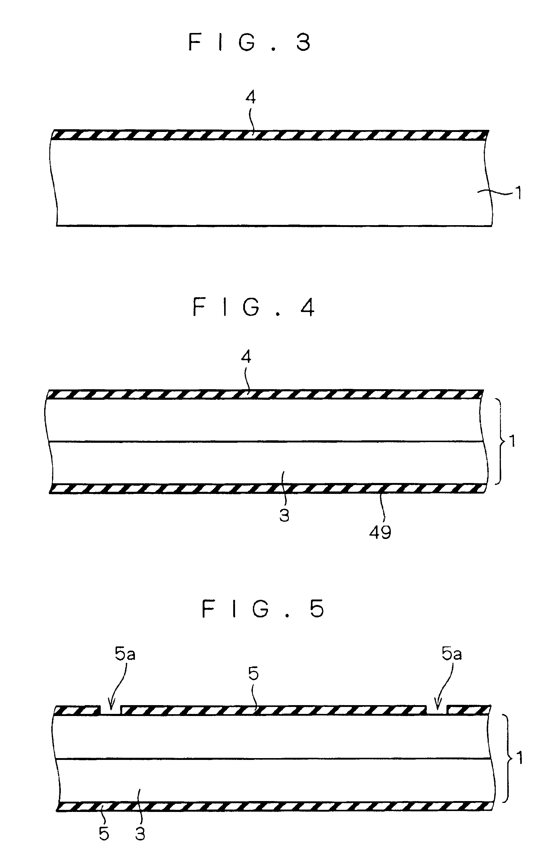
[0044]FIG. 1 is a plan vi...
PUM
 Abstract
Description
Claims
Application Information
 - R&D Engineer
- R&D Manager
- IP Professional
- Industry Leading Data Capabilities
- Powerful AI technology
- Patent DNA Extraction
Browse by: Latest US Patents, China's latest patents, Technical Efficacy Thesaurus, Application Domain, Technology Topic.
© 2024 PatSnap. All rights reserved.Legal|Privacy policy|Modern Slavery Act Transparency Statement|Sitemap