

Semiconductor device
a technology of semiconductor devices and semiconductor, which is applied in the details of semiconductor/solid-state devices, semiconductor devices, electrical apparatus, etc., can solve the problems of markedly lowering the production yield of semiconductor devices, and achieve the suppression of an increase in the length of wires, shortening the wire length, and suppressing the effect of wire sagging
Inactive Publication Date: 2005-01-04
RENESAS ELECTRONICS CORP
View PDF11 Cites 7 Cited by
- Summary
- Abstract
- Description
- Claims
- Application Information
AI Technical Summary
Benefits of technology
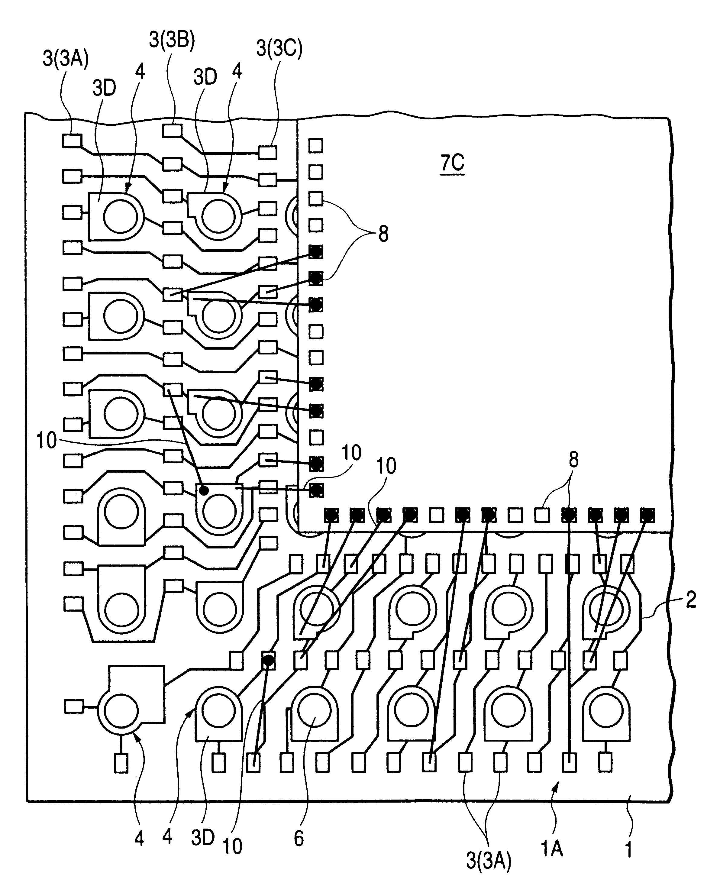
[0008]In the face up structure, a wire connecting pad is indispensable for interconnection, because an electrode formed on a circuit forming surface of a semiconductor chip and an interconnection formed on the chip mounting surface of a substrate are electrically connected via a conductive wire. Only one wire connecting pad is formed per interconnection, which does not cause a problem when an ordinarily-employed semiconductor chip of a predetermined external size is mounted. When a semiconductor chip has an external size smaller than that of an ordinary semiconductor chip, on the other hand, the length of the wire for connecting the electrode of the semiconductor chip with the wire connection pad of the interconnection increases with a decrease in the external size of the semiconductor chip, which worsens the sagging of the wire (sagging of the wire loop after bonding), leading to a tendency to cause inconveniences such as short-circuit between the wire and the interconnection in a wire bonding step for connecting the electrode of the semiconductor chip with the wire connecting pad of the interconnection via the wire. This tendency due to the worsening of the wire sagging is eminent particularly in the CSP type semiconductor, because the loop height (the height from the circuit forming surface of the semiconductor chip to the top portion perpendicular thereto) of the wire is lowered for making the semiconductor device thinner.
[0027]According to any one of the above-described means (1) to (4), when a semiconductor chip having an external size smaller than an ordinary semiconductor chip of a predetermined external size is integrated in a semiconductor, it is possible to select a proper wire connecting pad from those arranged from the peripheral side toward the inner side of the substrate so as to shorten the wire length according to the external size of the semiconductor chip, which makes it possible to suppress the wire length which otherwise increases with a decrease in the external size of the semiconductor chip. As a result, an increase in the inductance can be suppressed, which makes it possible to produce a semiconductor device without deteriorating its electrical properties even in the case where a semiconductor chip smaller in external size than an ordinary semiconductor chip is integrated in it.
Problems solved by technology
When a semiconductor chip has an external size smaller than that of an ordinary semiconductor chip, on the other hand, the length of the wire for connecting the electrode of the semiconductor chip with the wire connection pad of the interconnection increases with a decrease in the external size of the semiconductor chip, which worsens the sagging of the wire (sagging of the wire loop after bonding), leading to a tendency to cause inconveniences such as short-circuit between the wire and the interconnection in a wire bonding step for connecting the electrode of the semiconductor chip with the wire connecting pad of the interconnection via the wire.
In a step for sealing the semiconductor chip, wire and the like with a resin sealing body by the transfer molding method, the wire flow tends to be caused by the insulating resin injected under pressure, leading to inconveniences such as short-circuit between two adjacent wires.
Inconveniences as described above markedly lower a production yield of the semiconductor device having, integrated therein, a semiconductor chip having a smaller external size than an ordinary semiconductor chip having a predetermined external size.
Method used
View moreImage
Smart ImageViewing Examples

Examples
embodiment 2
[0049]FIG. 22 is a fragmentary plan view illustrating the semiconductor device of the present invention from which a resin sealing body has been removed;
embodiment 3
[0050]FIG. 23 is a plan view illustrating the substrate of the semiconductor device of the present invention; and
embodiment 4
[0051]FIG. 24 is a fragmentary cross-sectional view illustrating the semiconductor device of the present invention.
DESCRIPTION OF THE PREFERRED EMBODIMENTS
[0052]Embodiments of the present invention will be described more specifically with reference to accompanying drawings. In all the drawings illustrating the embodiments of the present invention, like elements having the same function will be identified by like reference numerals and overlapping description will be omitted.
Login to View More PUM
 Abstract
Provided is a technique which permits production of a semiconductor device having, integrated therein, a semiconductor chip smaller in external size than an ordinary semiconductor chip without lowering the production yield. The semiconductor device according to the present invention comprises a substrate having a square-shaped plane and having an interconnection formed on a first surface (chip mounting surface) of first and second opposite surfaces; a semiconductor chip which is mounted on the first surface of said substrate and has an electrode formed on a first surface (circuit forming surface) of first and second opposite surfaces of the semiconductor chip, and a conductive wire for electrically connecting the electrode of said semiconductor chip with the interconnection of said substrate, said interconnection having a plurality of connecting pads arranged from the peripheral side toward the inner side of said substrate.
Description
[0002]This is a continuation application of U.S. Ser. No. 09 / 495,918, filed Feb. 2, 2000 now U.S. Pat. No. 6,472,749.BACKGROUND OF THE INVENTION[0003]The present invention relates to a semiconductor device. In particular, the present invention relates to a technique effective when used for a semiconductor device having a face up structure.[0004]Semiconductor devices which are integrated in small-sized electronic equipment such as mobile phone, portable information processing terminal equipment or portable personal computer are requested to be thinner and smaller and have more pins. As semiconductor devices satisfying such requirements, CSP (Chip Size Package or Chip Scale Package) type ones have been developed for example. CSP type semiconductor devices having various structures have been proposed and already industrialized, but among them, those having a face up structure which can be produced at a low cost using an existing plant are most popular.[0005]The CSP type semiconductors ...
Claims
Login to View More Application Information
Patent Timeline
 IPC IPC(8): H01L23/31H01L23/28H01L23/48H01L23/498H01L23/12H01L21/60
CPCH01L23/3121H01L23/49838H01L24/32H01L24/49H01L24/45H01L2224/32225H01L2224/45144H01L2224/48091H01L2224/48095H01L2224/48227H01L2224/48465H01L2224/49171H01L2224/49175H01L2224/73265H01L2224/85201H01L2224/85205H01L2224/92247H01L2924/01004H01L2924/01013H01L2924/01014H01L2924/01029H01L2924/0105H01L2924/01079H01L2924/01082H01L2924/15183H01L2924/15311H01L2924/30107H01L2924/01006H01L2924/01019H01L2924/01023H01L2924/01033H01L24/48H01L2924/0132H01L2924/1517H01L2924/1579H01L2224/29111H01L2224/2919H01L2924/12041H01L2924/19107H01L2924/00014H01L2924/00012H01L2924/00H01L2224/13111H01L2924/0665H01L2924/0695H01L2924/181H01L2924/12042H01L2224/05554H01L24/73H01L2924/10162
InventorHIRANO, TSUGIHIKOOZAWA, HIDEMI
OwnerRENESAS ELECTRONICS CORP