Semiconductor laser and method for fabricating the same

a semiconductor laser and semiconductor technology, applied in semiconductor lasers, laser details, electrical equipment, etc., can solve the problems of difficult to obtain window structure and the inability of lasers to achieve high output, and achieve the effect of increasing fabrication costs and without lowering yield

Inactive Publication Date: 2010-06-15
PANASONIC CORP
View PDF14 Cites 0 Cited by
  • Summary
  • Abstract
  • Description
  • Claims
  • Application Information

AI Technical Summary

Benefits of technology

[0049]According to the semiconductor laser of this invention, a nitride semiconductor laser having a substantial window structure formed without modifying the basic structure thereof can be realized, and therefore, the COD can be suppressed in the nitride semiconductor laser without affecting other electric / optical characteristics. Also, in the fabrication method for the semiconductor laser, processing generally employed in the semiconductor process is merely additionally performed on a resonator end face as the end face treatment, and therefore, the nitride semiconductor laser in which the COD is suppressed can be fabricated without lowering the yield and increasing the fabrication cost.

Problems solved by technology

It is known that catastrophic optical damage (COD) is caused on a resonator end face in such a nitride semiconductor laser and thus prevents the laser from attaining high output in the same manner as in a conventional AlGaAs-based infrared semiconductor laser or a conventional AlGaInP-based red semiconductor laser.
In a nitride semiconductor, however, it is difficult to disorder a multiple quantum well, and hence, the window structure is difficult to obtain in the aforementioned manner.

Method used


Image

  • Semiconductor laser and method for fabricating the same
  • Semiconductor laser and method for fabricating the same
  • Semiconductor laser and method for fabricating the same

Examples


embodiment 1

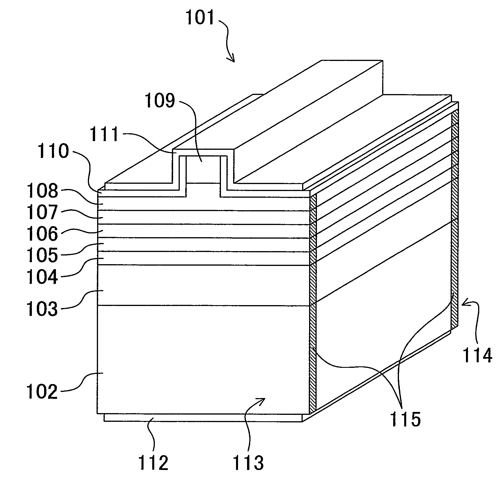
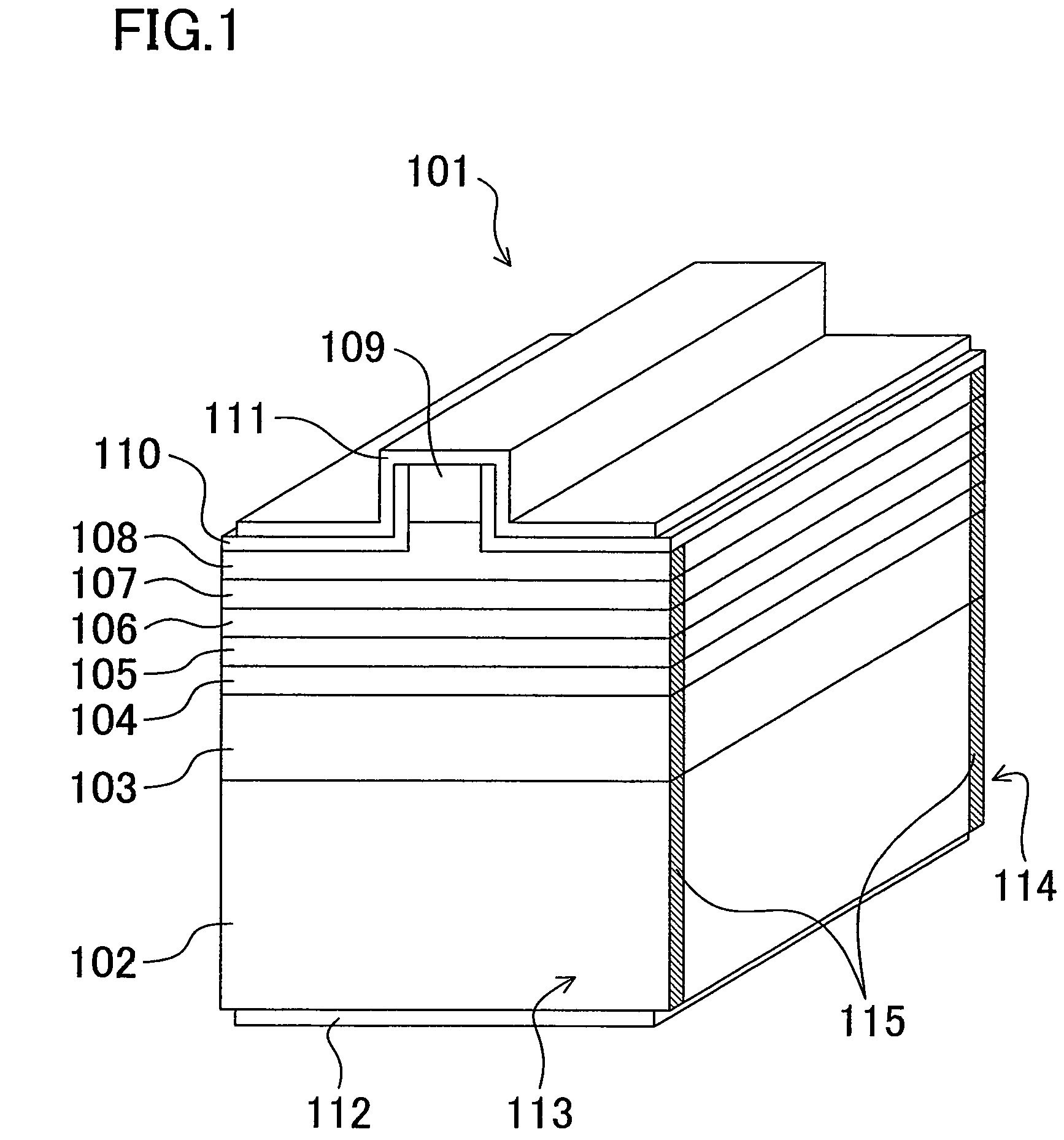
[0107]FIG. 1 is a perspective view of a semiconductor laser according to Embodiment 1 of the invention. The semiconductor laser 101 has an epitaxial layer structure in which a first cladding layer 103 made of Si-doped n-type (first conductivity type) Al0.05Ga0.95N (with a thickness of 1 μm and a carrier concentration of 5×1017 cm−3), a first guiding layer 104 made of Si-doped n-type GaN (with a thickness of 100 nm and a carrier concentration of 5×1017 cm−3), an active layer 105 of a multiple quantum well of a non-doped In0.08Ga0.92N well layer (with a thickness of 3 nm) and a GaN barrier layer (with a thickness of 8 nm), a second guiding layer 106 made of non-doped GaN (with a thickness of 100 nm), an overflow suppressing layer 107 made of Mg-doped p-type (second conductivity type) Al0.15Ga0.85N (with a thickness of 10 nm and a carrier concentration of 1×1019 cm−3), a second cladding layer 108 made of Mg-doped p-type Al0.1Ga0.9N / GaN superlattice (with a thickness of 500 nm) and a co...

embodiment 2

[0122]Embodiment 2 of the invention will now be described with reference to FIGS. 6A and 6B. In this embodiment, the active layer 105 of the semiconductor laser 101 shown in FIG. 1 is formed as an undoped GaN bulk (with a thickness of 100 nm) instead of the multiple quantum well. Also, the first guiding layer 104, the second guiding layer 106 and the overflow suppressing layer 107 are not formed. Apart from this, the semiconductor laser of this embodiment has a similar structure to that of Embodiment 1 and is fabricated in a similar fabrication method to that described in Embodiment 1.

[0123]Also in this embodiment, a window region for suppressing the COD is formed by introducing an impurity element with higher electronegativity than nitrogen, which will be described with reference to FIGS. 6A and 6B. FIGS. 6A and 6B respectively correspond to FIGS. 4A and 4B mentioned in Embodiment 1, and are energy band diagrams of a first cladding layer 601, an active layer 602 and a second claddi...

embodiment 3

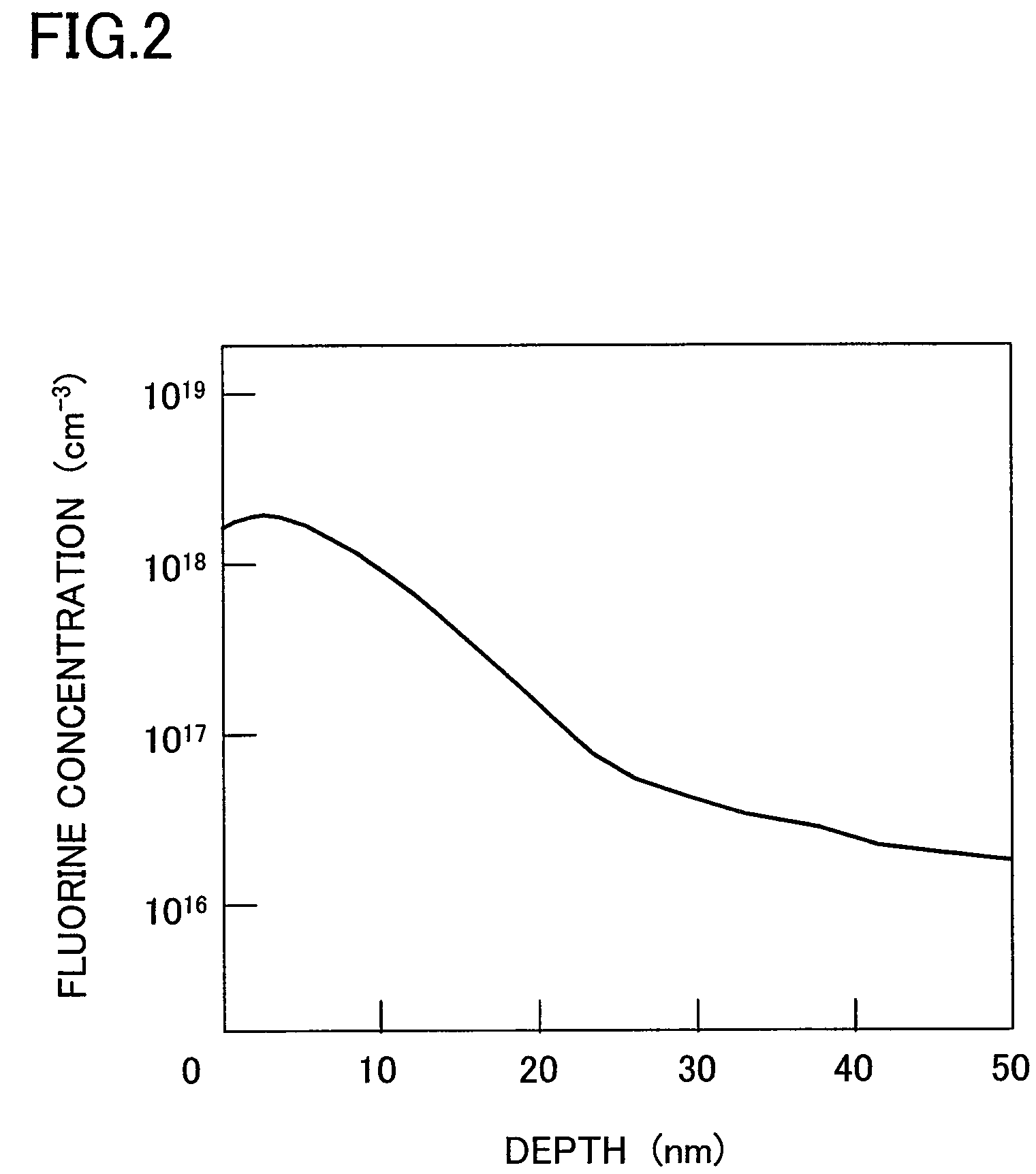
[0127]Embodiment 3 of the invention will now be described with reference to FIG. 7. This embodiment describes a fabrication method, in which the end face treatment is performed by a method other than the plasma processing, i.e., exposing an end face to plasma including an impurity element with higher electronegativity than nitrogen. Procedures other than the end face treatment are performed in the same manner as in Embodiment 1, and an impurity element with higher electronegativity than nitrogen such as fluorine is ion implanted through a resonator end face of a semiconductor laser having been processed into the shape of a bar having a resonator end face exposed through the cleavage. FIG. 7 corresponds to FIG. 2 mentioned in Embodiment 1 and shows the profile along the depth direction of the ion implanted fluorine. In this embodiment, the peak implantation amount is 6×1018 cm−3 and the implantation depth is 170 nm, and the implantation amount and the implantation depth of the ion im...


PUM


Abstract

A semiconductor laser (101) includes a first cladding layer (103), an active layer (105) and a second cladding layer (108). A window region (115) including fluorine, that is, an impurity element with higher electronegativity than nitrogen, is formed in the vicinity of a front end face (113) and a rear end face (114) of a laser resonator. The window region (115) is formed by exposing the front end face (113) and the rear end face (114) to carbon fluoride (CF4) plasma. The effective band gap of a portion of the active layer (105) disposed in the window region (115) is larger than the effective band gap of another portion of the active layer, and hence, it functions as an end face window structure for suppressing COD.

Description

RELATED APPLICATIONS[0001]This application is the U.S. National Phase under 35 U.S.C. §371 of International Application No. PCT / JP2007 / 063681, filed on Jul. 9, 2007, which in turn claims the benefit of Japanese Application No. 2006-208938, filed on Jul. 31, 2006, the disclosures of which Applications are incorporated by reference herein.TECHNICAL FIELD[0002]The present invention relates to a nitride semiconductor laser lasing at a wavelength ranging from a blue to UV region and used in an optical pickup or a solid-state lighting device and a method for fabricating the same, and more particularly, it relates to a surface treatment technique for a resonator end face for suppressing catastrophic optical damage.BACKGROUND ART[0003]A semiconductor laser included in an optical pickup used in reproducing / recording an optical disk attains a higher recording density in the optical disk as the lasing wavelength is shorter. Therefore, a nitride semiconductor laser lasing at a wavelength rangin...

Claims


Application Information

Patent Timeline
Patent Type & Authority Patents(United States)
IPC IPC(8): H01S5/00
CPCB82Y20/00H01S5/162H01S5/34333H01S5/0021H01S5/2009H01S5/305H01S5/3063H01S5/3404H01S5/2201
Inventor UEDA, DAISUKEYURI, MASAAKIHASEGAWA, YOSHIAKIMATSUDA, KENICHI
Owner PANASONIC CORP
Why Eureka
Try Eureka