Surface-emitting type semiconductor laser and method for manufacturing the same

a laser and surface-emitting technology, applied in the direction of lasers, semiconductor lasers, solid-state devices, etc., can solve the problems of ohmic contact, higher resistance, electrode peeled off, etc., and achieve the effect of sufficient ohmic contact, low resistance, and low yield

Inactive Publication Date: 2007-05-03
SEIKO EPSON CORP
View PDF4 Cites 2 Cited by
  • Summary
  • Abstract
  • Description
  • Claims
  • Application Information

AI Technical Summary

Benefits of technology

[0012] In accordance with an advantage of some aspects of the present invention, it is possible to provide a surface-emitting type semiconductor laser in which low resistance and sufficient ohmic contact can be achieved, and a method for manufacturing a surface-emitting type semiconductor laser that can manufacture the surface-emitting type semiconductor laser without lowering the yield.

Problems solved by technology

The electrode may need to be formed on a lower composition layer with a smaller aluminum (Al) composition among the layers composing the above-described DBR that is formed with an AlGaAs group material, because it is difficult to have ohmic contact with a higher composition layer with a higher aluminum (Al) composition.
If an electrode is formed on the GI layer, sufficient ohmic contact cannot be obtained, which leads to a problem of higher resistance.
Also, because the electrode formed on the GI layer has poor adhesion with the GI layer, there is a possibility that the electrode may be peeled off during the mounting process, and the yield may be lowered.
However, when a portion above the thick film layer is formed into a columnar configuration, a stress may be generated at a base section of the columnar section, and cracks may occur in the base section; and if the active layer is disposed at the base section, the characteristics of the element may be deteriorated.

Method used


Image

  • Surface-emitting type semiconductor laser and method for manufacturing the same
  • Surface-emitting type semiconductor laser and method for manufacturing the same
  • Surface-emitting type semiconductor laser and method for manufacturing the same

Examples


Embodiment Construction

[0043] A surface-emitting type semiconductor laser and its manufacturing method in accordance with an embodiment of the invention are described in detail with reference to the accompanying drawings. It is noted that the embodiment to be described below indicates a part of modes of the invention, does not limit the invention, and can be appropriately modified within the scope of the invention. Also, in the drawings referred to below for describing the invention, the scale may be changed for each of the layers and each of the members such that the layers and the members can have appropriate sizes that can be recognized on the drawings.

[0044] Surface-Emitting Type Semiconductor Laser

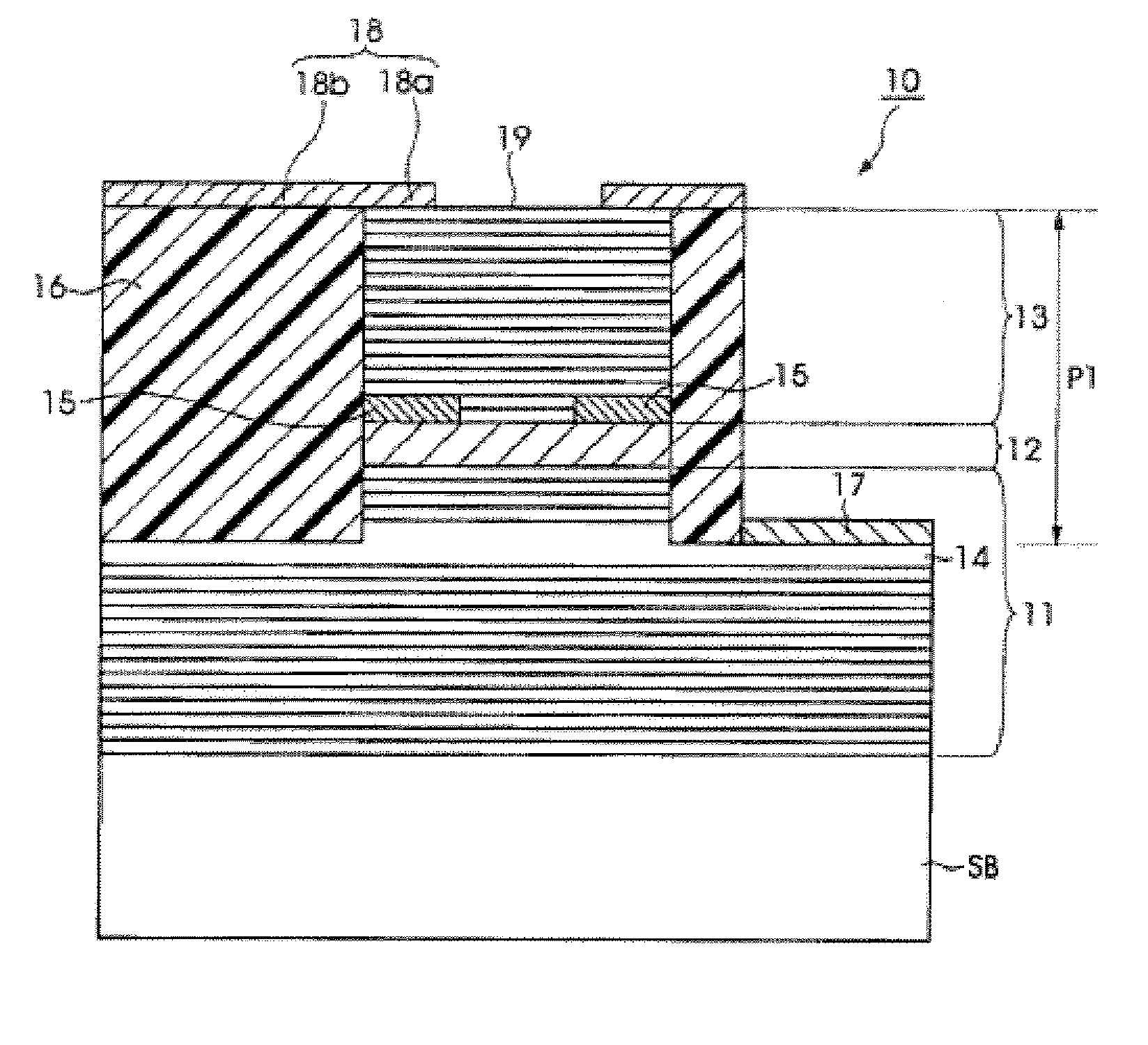
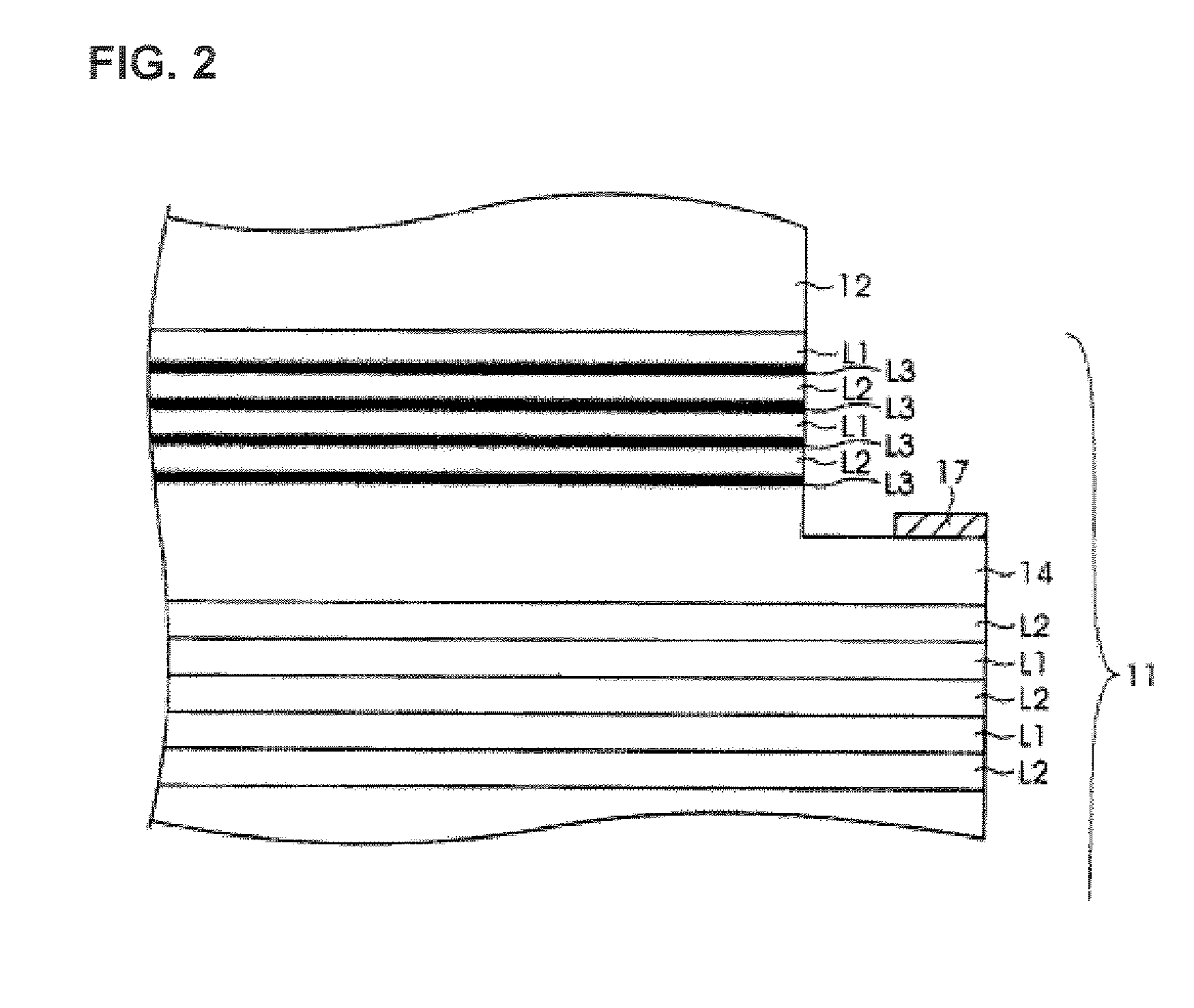
[0045]FIG. 1 is a schematic cross-sectional view of a surface-emitting type semiconductor laser 10 in accordance with an embodiment of the invention. As shown in FIG. 1, the surface-emitting type semiconductor laser 10 is formed on a semiconductor substrate (e.g., an n-type GaAs substrate in the present e...


PUM


Abstract

A surface-emitting type semiconductor laser includes: an upper mirror and a lower mirror each composed of alternately formed first semiconductor layers and second semiconductor layers; an active layer disposed between the upper mirror and the lower mirror, wherein the surface-emitting laser emits laser light in a direction in which the first semiconductor layers and the second semiconductor layers are formed; a thick film layer formed with one of the first semiconductor layers composing the lower mirror, the thick film layer being thicker than other of the first semiconductor layers; and a third semiconductor layer provided between the thick film layer and one of the second semiconductor layers on the thick film layer, the third semiconductor layer having a refractive index between a refractive index of the first conductive layer and a refractive index of the second semiconductor layer.

Description

[0001] The entire disclosure of Japanese Patent Application No. 2005-319278, filed Nov. 2, 2005 is expressly incorporated by reference herein. BACKGROUND [0002] 1. Technical Field [0003] The present invention relates to surface-emitting type semiconductor lasers that emit laser light and methods for manufacturing the same. [0004] 2. Related Art [0005] A surface-emitting type semiconductor laser is provided with a resonator formed in a direction orthogonal to a substrate surface, and emits laser light from the substrate surface. Compared to edge-emitting type semiconductor lasers that use parallel cleavage planes of a substrate as a resonator, surface-emitting type semiconductor lasers have various favorable characteristics. For example, surface-emitting type semiconductor lasers are suitable for mass-production, capable of direct modulation, and capable of operation with low threshold current, and a two-dimensional laser array structure can be readily formed with surface-emitting ty...

Claims


Application Information

Patent Timeline
Patent Type & Authority Applications(United States)
IPC IPC(8): H01L33/00H01S5/183H01S5/343
CPCB82Y20/00H01S5/0422H01S5/0425H01S5/18311H01S5/18341H01S5/18347H01S5/3432H01S2301/176H01S5/04257
Inventor KANEKO, TSUYOSHI
Owner SEIKO EPSON CORP
Why Eureka
Try Eureka