
Semiconductor device, designing method and designing device thereof

a technology of semiconductor/solid-state devices and design methods, applied in semiconductor/solid-state device testing/measurement, instruments, basic electric elements, etc., can solve problems such as yield reduction, and achieve the effect of alleviating density differences and reducing density differences

Inactive Publication Date: 2005-01-04
RENESAS ELECTRONICS CORP
View PDF8 Cites 9 Cited by
  • Summary
  • Abstract
  • Description
  • Claims
  • Application Information

AI Technical Summary

Benefits of technology

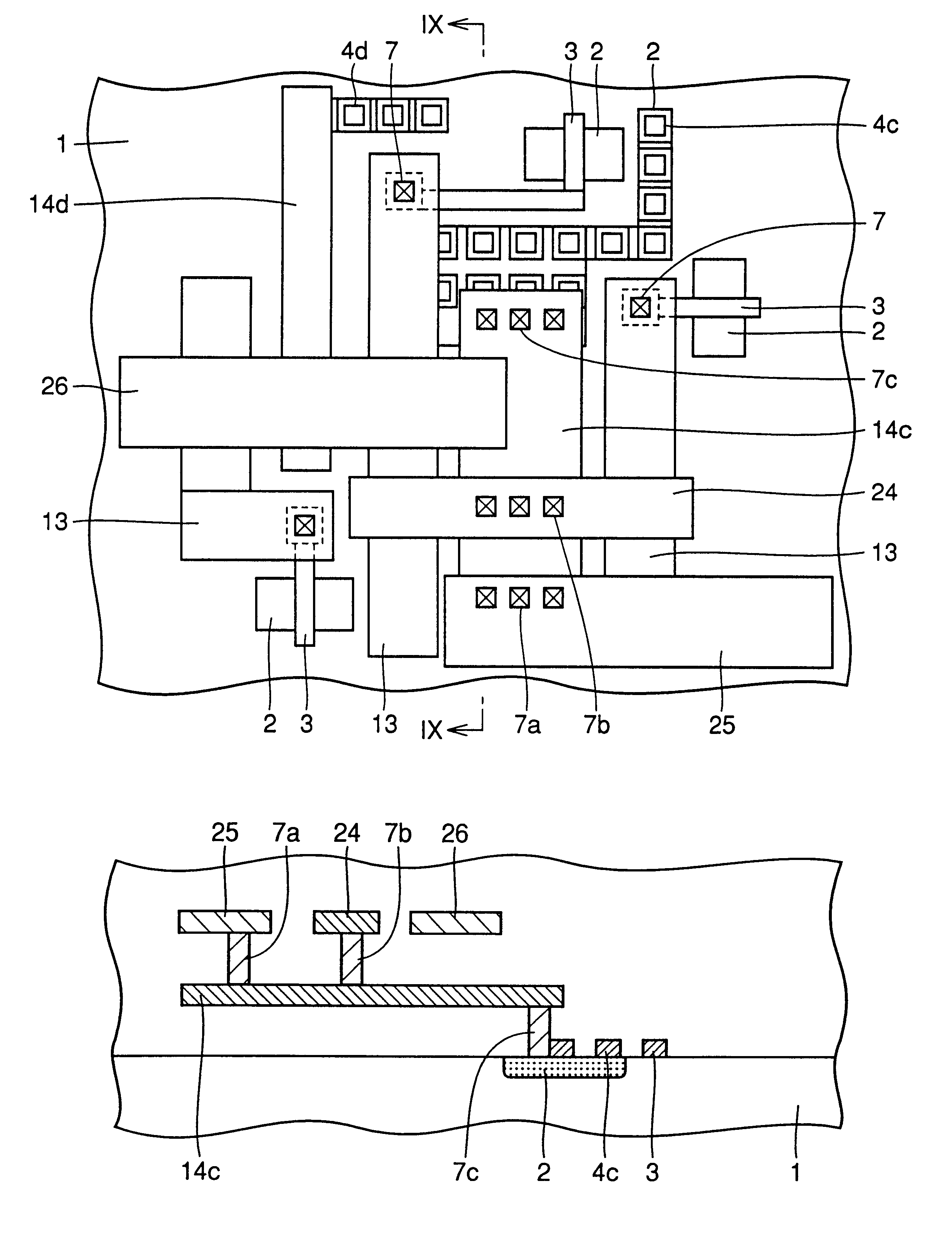
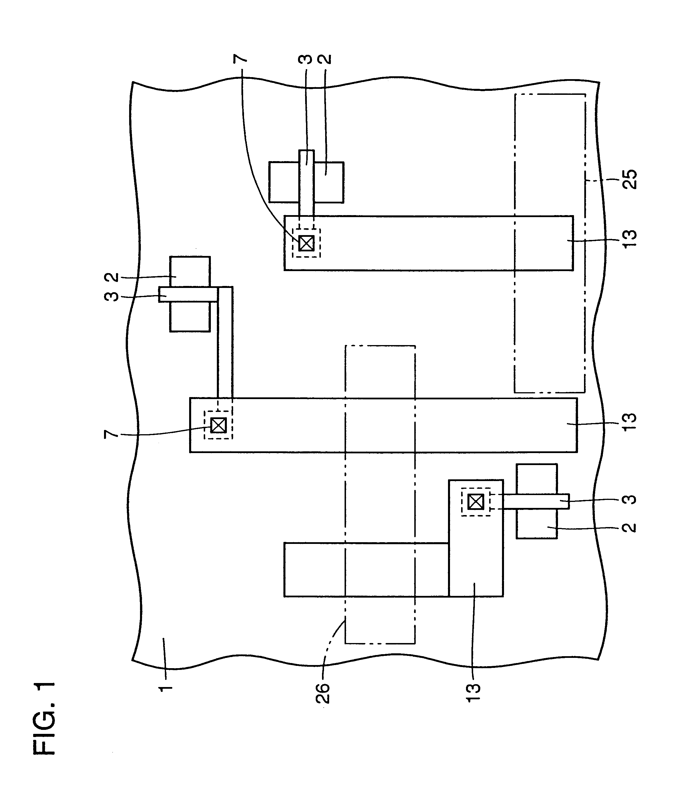
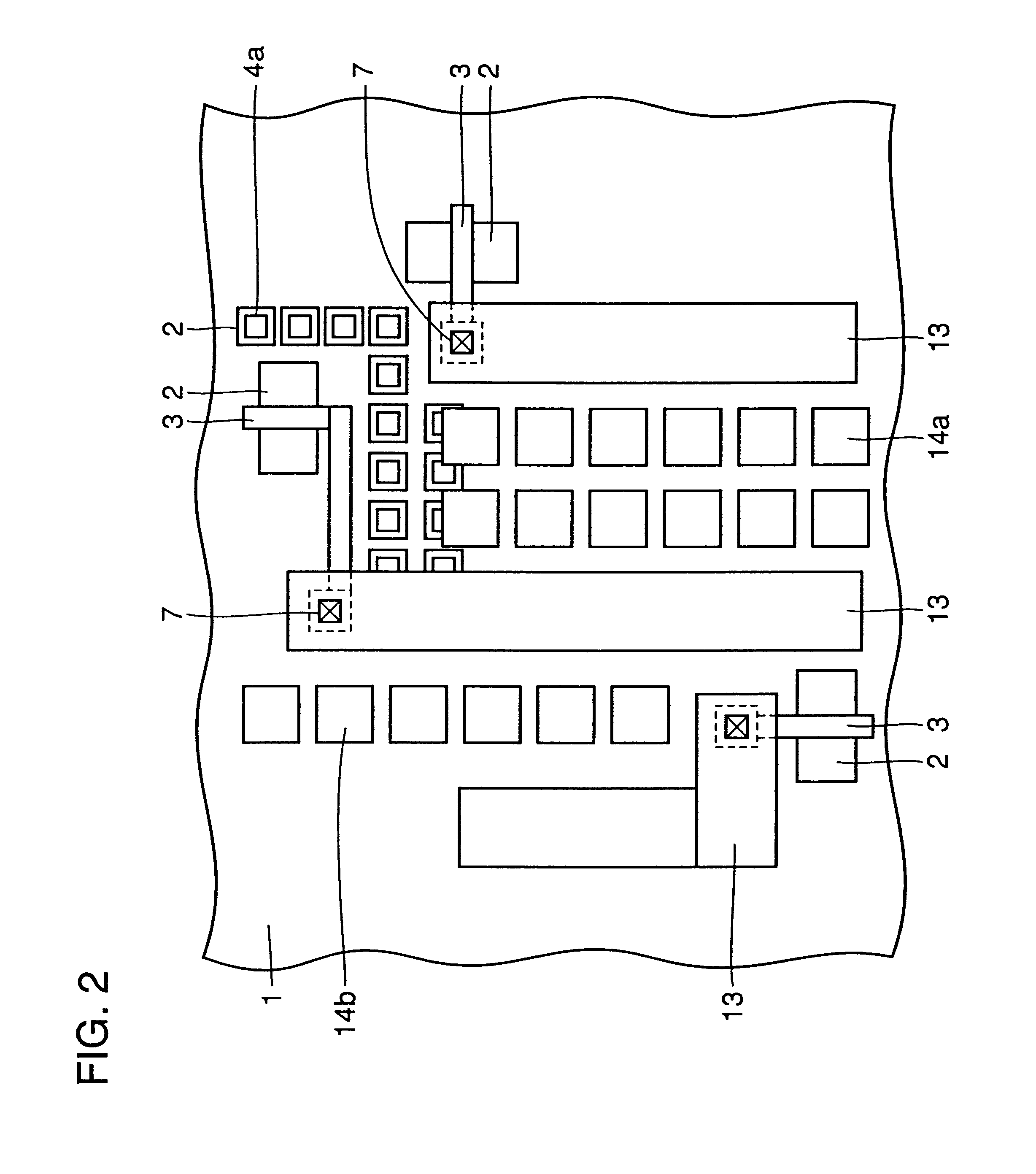
In order to achieve the above-mentioned objective, in one aspect of the present invention, a semiconductor device, which is manufactured through a photolithographic technique, is provided with a dummy pattern that is installed so as to alleviate the difference in density so that degradation in the patterning precision occurring at a thinner portion at the time of exposure due to the difference in density is eliminated. The application of this arrangement alleviates the difference in density by installing the dummy pattern so that it becomes possible to prevent the phenomenon that causes degradation in the patterning precision in the photolithographic technique.
The application of the above-mentioned arrangement enables a designing process in which the layout of dummy patterns and the electrical connection from the respective dummy patterns either to the power-supply wire or to the ground wire are effectively placed.

Problems solved by technology

In the case of the production of such fine wiring, this problem has come to cause a reduction in the yield, and can not be neglected.

Method used


Image

  • Semiconductor device, designing method and designing device thereof
  • Semiconductor device, designing method and designing device thereof
  • Semiconductor device, designing method and designing device thereof

Examples


first embodiment

(First Embodiment)

As illustrated in FIG. 13, in order to prevent degradation in the patterning precision occurring at a thin portion at the time of exposure in the photolithographic printing technique, a dummy pattern 54 is inserted to a thin portion in a mask 5 of each of wiring layers so as to alleviate a difference in density.

In the pattern of the mask 5, the dummy pattern 54 is inserted to each thin portion so that the pattern is seemingly free from the difference in density; thus, the degree of the occurrence of light diffraction is reduced to be the same as that of a dense portion, and it is possible to prevent degradation in the patterning precision.

second embodiment

(Second Embodiment)

In a conventional method, with respect to a flow of processes in a CAD (Computer Aided Design) system for designing a semiconductor device, a design rule check (DRC) is conducted after a layout designing job. The DRC is a process for checking to see whether or not a wiring layout conforms to a predetermined manufacturing standard. Next, the wiring layout, obtained through a design, is subjected to a layout vs schematic (LVS) process to check to see whether it matches with the circuit diagram of an originally expected circuit. Then, calculations are carried out with respect to the capacitance and resistance of the wiring.

A layout design of a dummy pattern to be added to wiring is carried out efficiently by using a mask generation CAD system, or the like.

Here, in order to generate a mask, a method is proposed in which a flow of jobs in a conventional designing CAD system is used as it is, and the designing data thus obtained is transferred to the mask generation CAD...

third embodiment

(Third Embodiment)

A memory medium in accordance with the third embodiment of the present invention is a memory medium in which a program described in the second embodiment is stored.

The application of this allows a computer to read and execute the program so that the load imposed on the operator can be reduced, and the above-mentioned designing method can be carried out accurately at high speeds.


PUM


Abstract

A semiconductor device is provided with dummy patterns at an originally thinner portion of each of layers, and each of these dummy patterns is electrically connected to a reference wire that is either a power-supply wire or a ground wire.

Description

BACKGROUND OF THE INVENTION1. Field of the InventionThe present invention relates to a semiconductor device and a designing method thereof, and also concerns a designing device for carrying out such a designing method.2. Description of the Background ArtIn general, in a manufacturing process of a semiconductor device, a photolithographic printing technique is sometimes used. More specifically, as illustrated in FIG. 17, a mask 5 having a predetermined pattern is formed on a removable layer 6, and light is directed to this so that a portion of the removable layer 6 that is not covered with the mask 5 is denatured and removed therefrom.In this case, however, when there is a difference in the density depending on the portions of the pattern of the mask 5 as illustrated in FIG. 17, at a thin portion, light tends to farther proceed to reach the rear side of the mask 5 due to the occurrence of light diffraction, interference, etc., resulting in degradation in the precision of the resultan...

Claims


Application Information

Patent Timeline
Patent Type & Authority Patents(United States)
IPC IPC(8): H01L23/544H01L23/52H01L23/528H01L27/02H01L21/3205G06F17/50H01L21/82H01L21/822H01L27/04
CPCH01L22/34H01L23/528H01L27/0207H01L2924/0002H01L2924/00H01L21/82
Inventor ITOH, NIICHI
Owner RENESAS ELECTRONICS CORP
Learn More