Light emitting diode with nanoparticles

Inactive Publication Date: 2005-01-04
TRANSPACIFIC IP LTD
View PDF7 Cites 52 Cited by
  • Summary
  • Abstract
  • Description
  • Claims
  • Application Information

AI Technical Summary

Problems solved by technology

However, emitting layer of a typical LED is formed by epitaxially growing; therefore, the growing speed is very slow.
Thus, the forming speed

Method used


Image

  • Light emitting diode with nanoparticles
  • Light emitting diode with nanoparticles
  • Light emitting diode with nanoparticles

Examples


Embodiment Construction

The following descriptions of the preferred embodiments are provided to understand the features of the present invention.

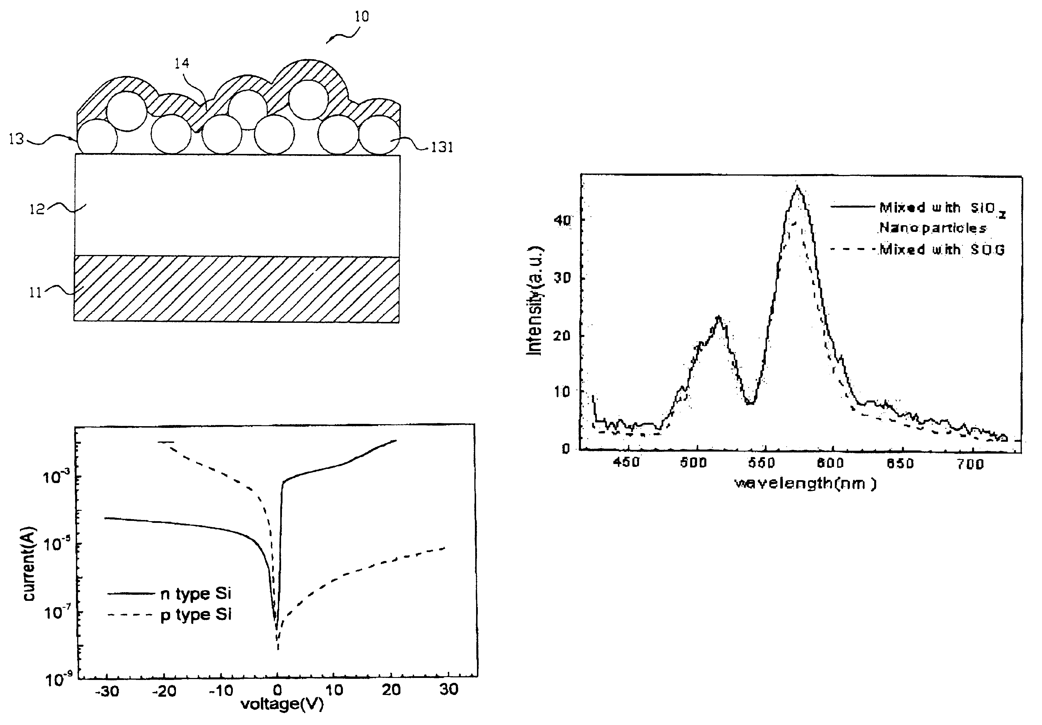
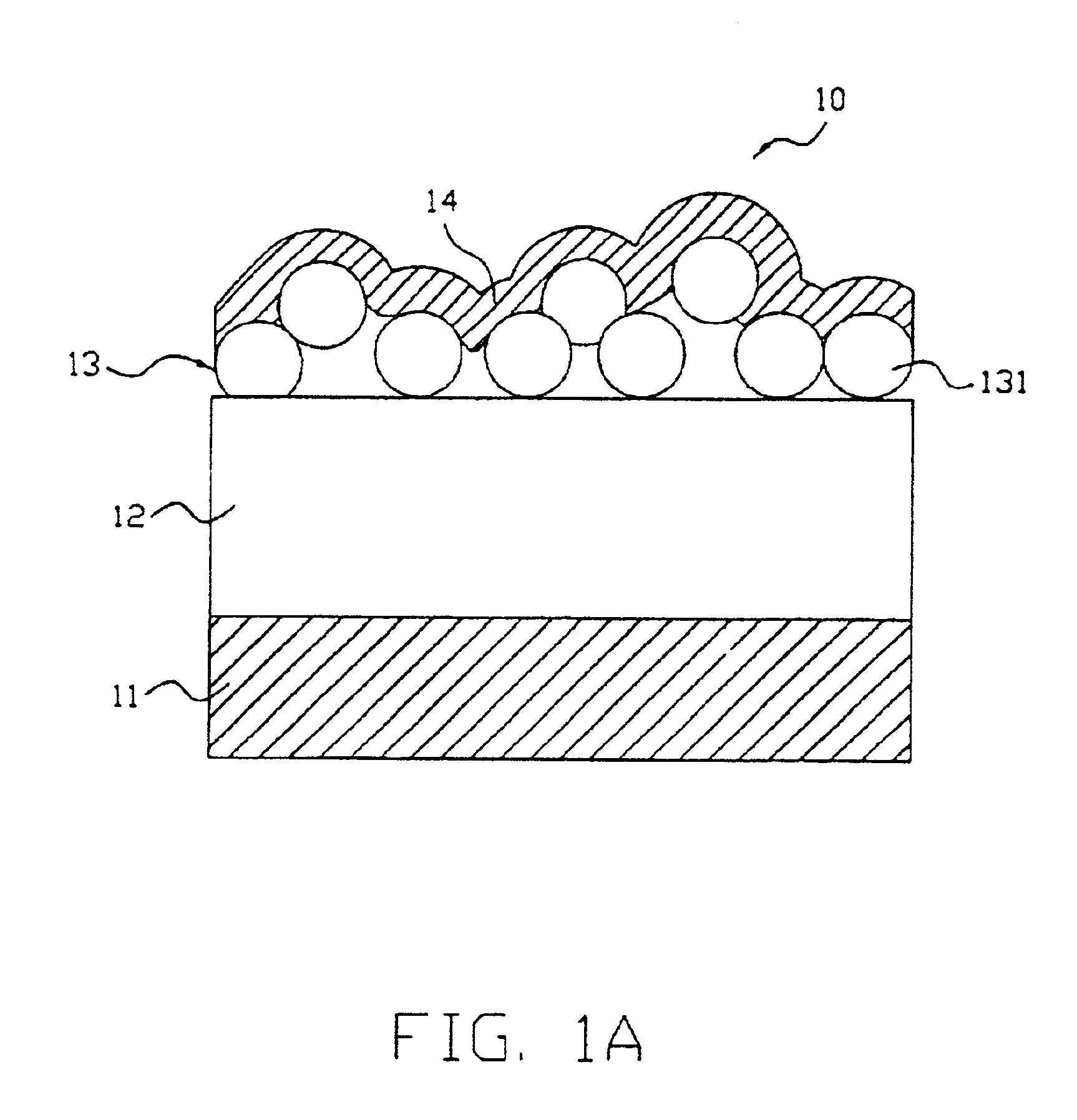
The present invention provides a light emitting diode (LED) with nanoparticles 10, please referring to the FIG. 1A, which comprises a first electrode 11 for electric conduction a substrate 12 for said LED to be grown thereon, a luminescent nanoparticles layer 13 for emitting light, and a second electrode 14 for electric conduction. Wherein said first electrode 12 may be an N-type electrode or a P-type electrode made by metal material, such as Au, Ag, Al, or Mg. Said substrate 12 may be a semiconductor substrate or an insulator substrate, typically, said substrate 12 is a silicon substrate. Similarly, said second electrode 14 may be an N-type electrode or a P-type electrode that is different to said first electrode 11, made by metal material, such as Au, Ag, Al, or Mg. Furthermore, said luminescent nanoparticles layer 13 substantially is an oxide luminescent nanopa...


PUM


Abstract

The present invention discloses a simple, low cost method to fabricate light emitting source using luminescent colloid nanoparticles. It uses monodispersed colloid light emitting nanoparticles of oxides, semiconductors, and polymers to fabricate high quality, narrow bandwidth light emitting source. The colloid particles can be dispersed homogeneously in liquid that can be coated easily on a substrate using a simple coating method such as spray, dip coating or spin coating. There is no restriction on the size or shape of the substrate. Therefore, a low cost, large area, high efficiency and reproducible light emitting source can be made easily.

Description

FIELD OF THE INVENTIONThe invention herein relates to a light emitting diode (LED), particularly, relates to a LED with nanoparticles.BACKGROUND OF THE INVENTIONRecently, the epitaxy technique is getting more and more improved, so it is very possible to have a double heterostructure with excellent quality, and which may provide LED more than 90% quantum efficiency. However, emitting layer of a typical LED is formed by epitaxially growing; therefore, the growing speed is very slow.Low-dimensional structures including nanoparticles or quantum dots (QDs) are supposed to provide significant enhancement in the density of states, so it increases the probability of light emission. Those low-dimensional structures can be epitaxially grown on bulk materials like GaAs wafers or separately formed by chemical methods.Luminescent nanoparticles formed by chemical methods have many advantages. First, it can be dissolved in the solvent to become a solution. Second, it can be applied on any substrat...

Claims


Application Information

Patent Timeline
IPC IPC(8): H01L33/00B82B1/00B81B1/00C09K11/06C09K11/56H01L33/08H01L33/28H01L51/50H05B33/02H05B33/14H05B33/26
CPCH01L33/08Y10S362/80H01L33/28
Inventor SU, WEI-FANGLIN, CHING-FUH
Owner TRANSPACIFIC IP LTD
Why Eureka
Try Eureka