

Printed-wiring substrate and method for fabricating the same
- Summary
- Abstract
- Description
- Claims
- Application Information
AI Technical Summary
Benefits of technology
Problems solved by technology
Method used
Image

Examples
third embodiment
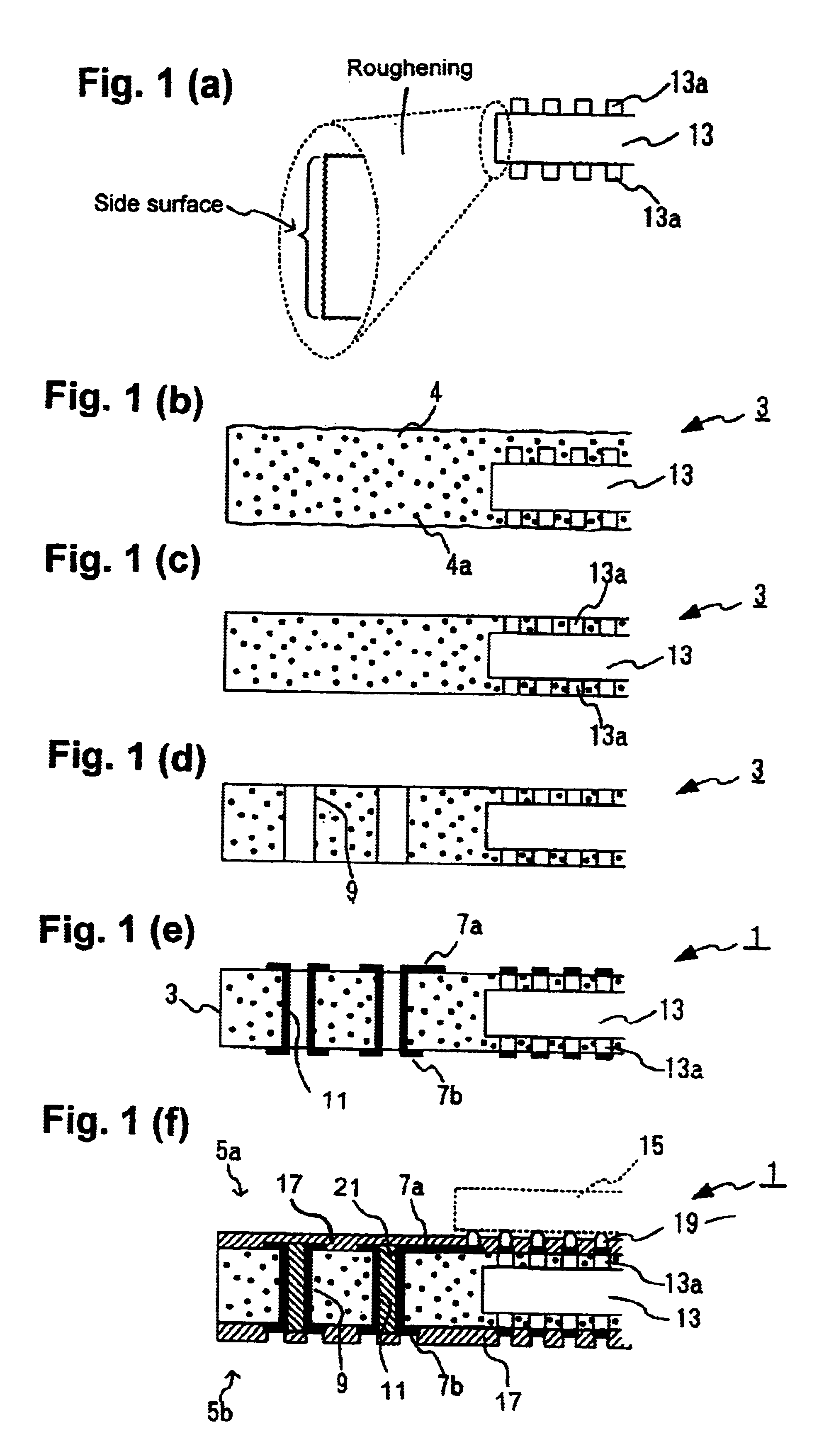
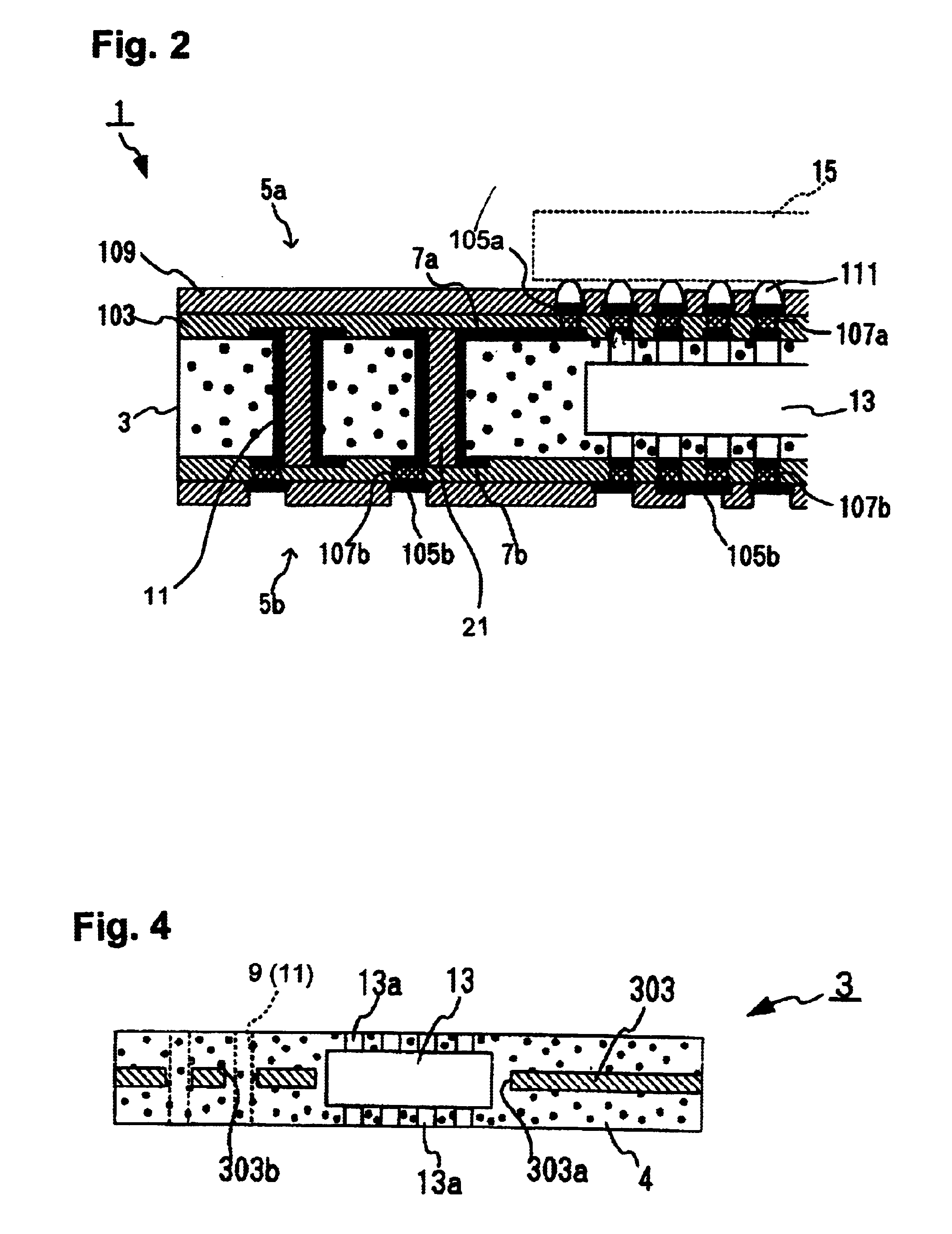
In addition to the above-described effects (1) to (3), the printed-wiring substrate achieves the following effects (4) to (7).
(4) Since the insulating substrate 3 is formed through alternate stacking of the resin 4 and the glass cloth 203 in the thickness direction thereof, the dimensional stability (i.e., stability of the substrate dimensions against temperature variation) and rigidity of the insulating substrate 3 can be improved, and the capacitor element embedded in the insulating substrate 3 can be protected effectively.
(5) The increased dimensional stability of the insulating substrate 3 enables the wiring patterns 7a and 7b and the second wiring patterns 105a and 105b to be formed on the insulating substrate 3 more accurately by the buildup process.
(6) The increased rigidity stability of the insulating substrate 3 enables fabrication of a large number of printed-wiring substrates 1 from a large substrate for multi-piece fabrication. As a result, the number of fabrication ste...
PUM
| Property | Measurement | Unit |
|---|---|---|
| Thickness | aaaaa | aaaaa |
| Size | aaaaa | aaaaa |
| Adhesion strength | aaaaa | aaaaa |
Abstract
Description
Claims
Application Information