PIN photodiode

a photodiode and pin technology, applied in the field of pin photodiodes, can solve the problems of parasitic effect that increases the electrostatic capacitance of the element and deteriorates the high-speed operating property of the diode element, and achieves the effect of suppressing the increase in the electrostatic capacitance of the photodiod

Inactive Publication Date: 2005-01-11
SAMSUNG ELECTRONICS CO LTD
View PDF2 Cites 5 Cited by
  • Summary
  • Abstract
  • Description
  • Claims
  • Application Information

AI Technical Summary

Benefits of technology

The present invention provides a PIN photodiode, which has an improved property as a high-speed light-receiving element through a control of the lateral depletion level of a bonding layer, thus suppressing an increase in the electrostatic capacitance in the photodiode.

Problems solved by technology

In the above PIN diode, if a negative electric field is applied to the P+ bonding layer through the electrode pad, the bonding is laterally extended as compared to the case in which no electric field is applied, so that the area of the P+ bonding layer increases, thus causing a parasitic effect that increases the electrostatic capacitance of the element.
However, as the electrostatic capacitance increases the RC time constant also increases, thereby deteriorating the high-speed operating property of the diode element.

Method used


Image

  • PIN photodiode
  • PIN photodiode
  • PIN photodiode

Examples


Embodiment Construction

Hereinafter, preferred embodiments of the present invention will be described with reference to the accompanying drawings. For the purposes of clarity and simplicity, a detailed description of known functions and configurations incorporated herein will be omitted as it may make the subject matter of the present invention unclear.

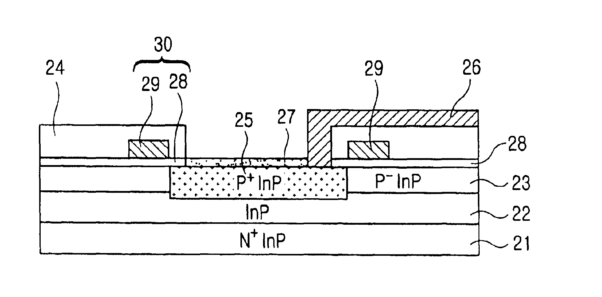
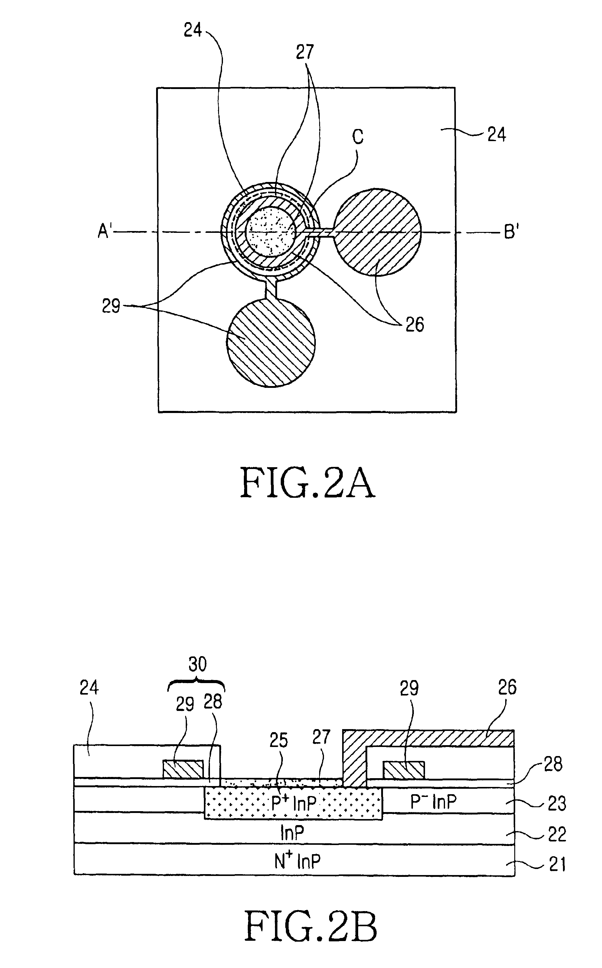
FIG. 2a is a top plan view of a PIN photodiode in accordance with an embodiment of the present invention, and FIG. 2b is a cross-sectional view taken along the line A′-B′ of FIG. 2a.

As shown in FIGS. 2a and 2b, the PIN photodiode in accordance with the present embodiment includes: an InP layer 22, which is a non-doped intrinsic semiconductor layer, a P− InP layer 23, a donut-shaped SiN insulation layer 24 with a circular window formed in the center part thereof, a P+ bonding layer 25 formed on the InP layer 22 within the circular window, an electrode pad 26 formed on the P+ bonding layer 25, and a SiN anti-reflection layer 27 formed on the P+ InP layer 25. ...


PUM


Abstract

Disclosed is a PIN photodiode used for a light-receiving element for optical communication. The PIN photodiode comprises a gate electrode structure consisting of a gate insulation layer and a gate electrode pad which prevent a bonding layer from being excessively depleted in the lateral direction at the time of applying a negative electric voltage to an electrode that is in contact with the bonding layer. The PIN photodiode allows the control of the electrostatic capacitance of the element by controlling the depletion level of the bonding layer in the lateral direction using the gate electrode pad. Therefore, it is possible to suppress the increase of the electrostatic capacitance and to achieve a high-speed operating property.

Description

CLAIM OF PRIORITYThis application claims priority to an application entitled “PIN Photodiode,” filed with the Korean Intellectual Property Office on Dec. 5, 2002 and assigned Serial No. 2002-76967, the contents of which are hereby incorporated by reference.BACKGROUND OF THE INVENTION1. Field of the InventionThe present invention relates to a PIN photodiode used for the reception of light signals in an optical communication field.2. Description of the Related ArtIn general, a PIN photodiode comprises a P-type semiconductor, a N-type semiconductor, and an intrinsic semiconductor layer interposed there-between. The PIN photodiode is typically used as a light-receiving element for converting an optical signal into an electric signal as it possessesexcellent characteristics in converting incident photons into electrons, mainly due to its ability to increase the width of a depletion layer of the PIN photodiode.FIG. 1a is a top plan view of a conventional PIN photodiode, and FIG. 1b is a c...

Claims


Application Information

Patent Timeline
Patent Type & Authority Patents(United States)
IPC IPC(8): H01L21/00H01L31/102H01L31/072H01L31/10H01L31/0336H01L31/06H01L31/0264H01L31/0328H01L31/109
CPCH01L31/105H01L31/022416H01L31/10
Inventor KANG, HWA-YOUNG
Owner SAMSUNG ELECTRONICS CO LTD
Why Eureka
Try Eureka