Fully-depleted SOI MOSFETs with low source and drain resistance and minimal overlap capacitance using a recessed channel damascene gate process

a damascene gate and fully-depleted technology, applied in the field of semi-detachable soi mosfets with can solve the problems of hammering the use of thin-film soi mosfets in semiconductor integrated circuits, and achieve excellent short-channel effects, low source and drain resistance, and minimal overlap capacitance

Inactive Publication Date: 2005-01-11
GLOBALFOUNDRIES US INC
View PDF19 Cites 67 Cited by
  • Summary
  • Abstract
  • Description
  • Claims
  • Application Information

AI Technical Summary

Benefits of technology

The present invention provides a technique for the fabrication of sub-0.05 μm channel length fully-depleted SOI MOSFET devices that exhibit excellent short-channel effects, low source and drain resistance and minimal overlap capacitance. The inventive technique utilizes a damascene-gate process which allows self-aligned thinning of a top Si-containing layer (i.e., SOI layer) of an SOI structure in the channel region to minimize short-channel effects while simultaneously maintaining thick SOI source and drain regions to permit formation of a low sheet resistance silicide layer. By utilizing a thin nitride layer deposition technique during the inventive method to form thin inner nitride spacers in the structure, the overlap capacitance between the gate and the source and drain regions is minimized.

Problems solved by technology

Over the past twenty-five years or so, the primary challenge of very large scale integration (VLSI) has been the integration of an ever-increasing number of metal oxide semiconductor field effect transistor (MOSFET) devices with high yield and reliability.
Despite the known advantages with thin film SOI technology, processing challenges exist which substantially hamper the use of thin film SOI MOSFETs in semiconductor integrated circuits.
For example, prior art processes for fabricating thin film SOI MOSFETs have difficulty in forming a thin (20 nm or less) SOI channel region, while simultaneously being able to maintain abutting thick SOI source and drain regions.

Method used


Image

  • Fully-depleted SOI MOSFETs with low source and drain resistance and minimal overlap capacitance using a recessed channel damascene gate process
  • Fully-depleted SOI MOSFETs with low source and drain resistance and minimal overlap capacitance using a recessed channel damascene gate process
  • Fully-depleted SOI MOSFETs with low source and drain resistance and minimal overlap capacitance using a recessed channel damascene gate process

Examples


second embodiment

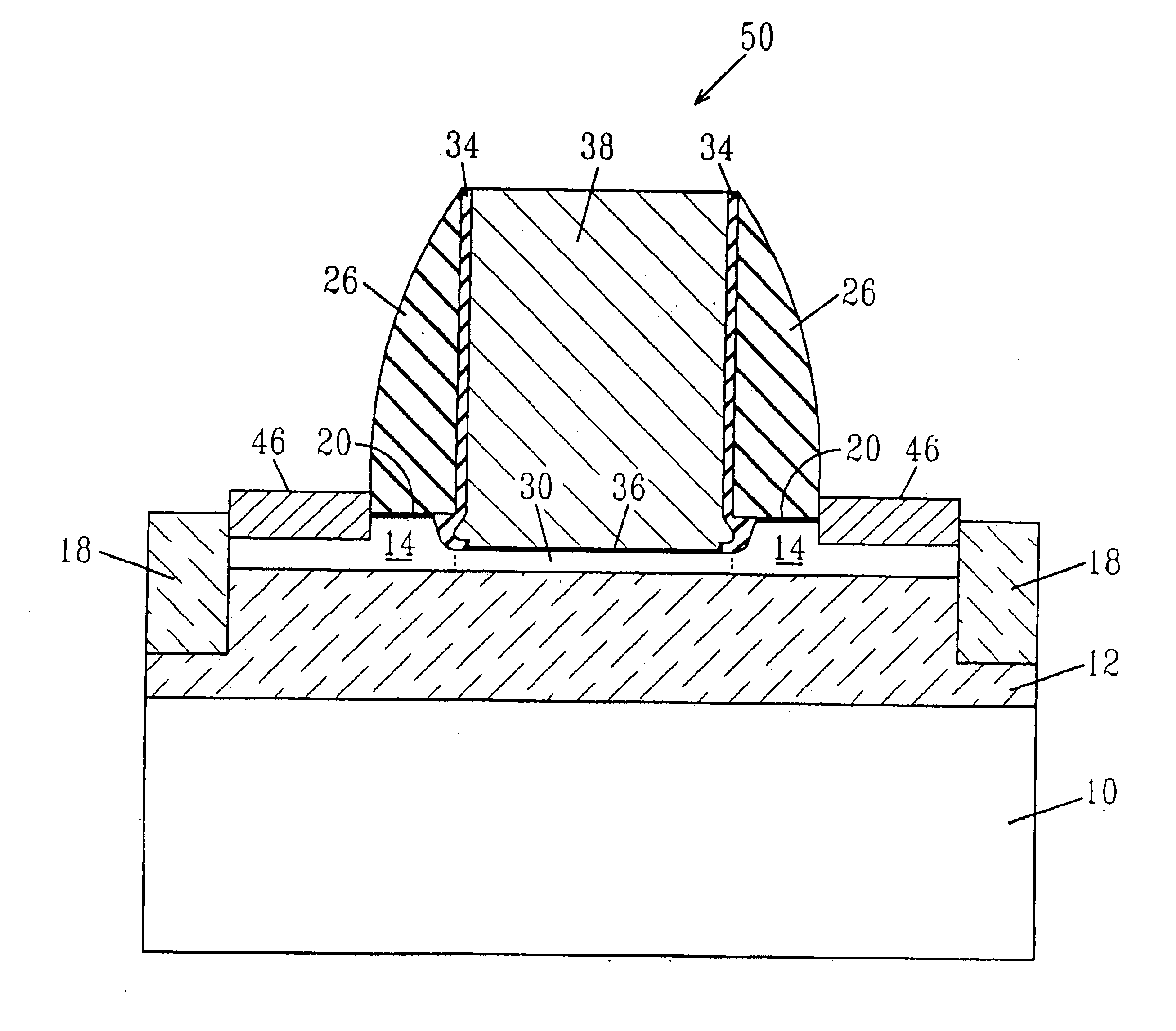
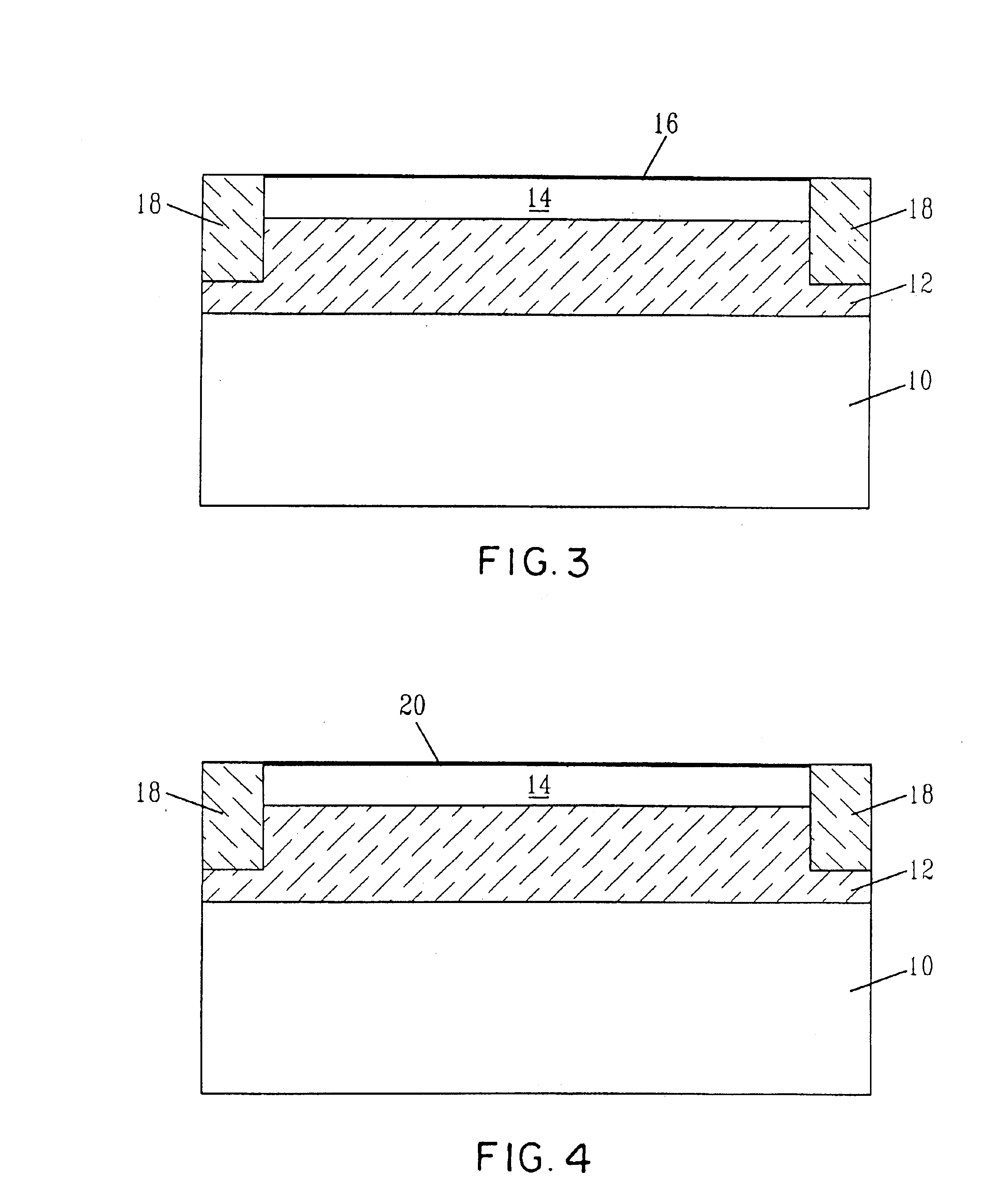
The first embodiment of the present invention (See, FIGS. 1-13), in which the * source / drain regions as well as the halo implant regions and the extension implant regions are formed after the gate region has been fabricated in the structure will be described first. the present invention (See, FIGS. 14-23) wherein the various implant regions are formed in the SOI layer prior to formation of the gate region will be described later.

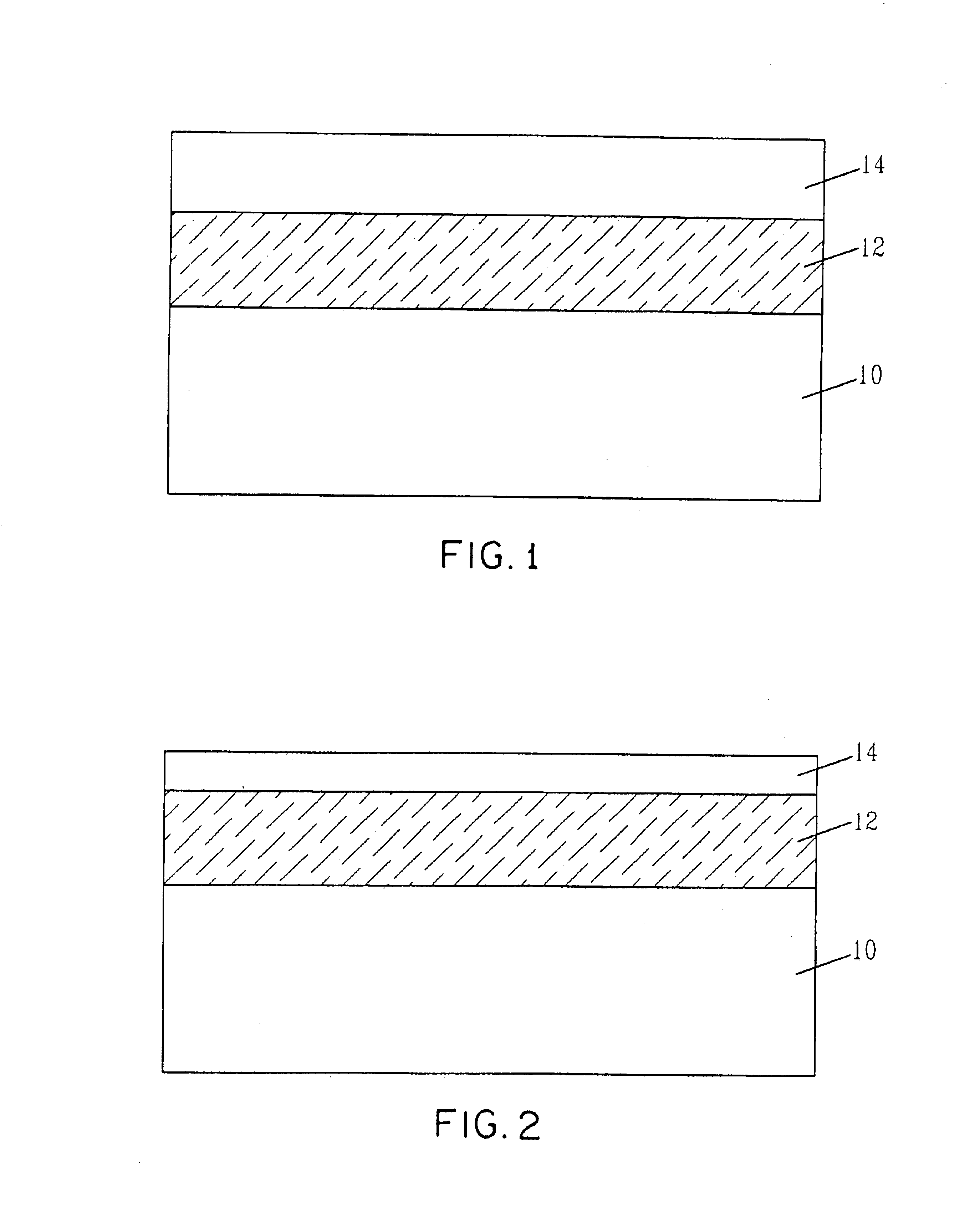
Reference is first made to FIG. 1 which illustrates an initial SOI structure that can be employed in the present invention. Specifically, the SOI structure shown in FIG. 1 comprises bottom Si-containing layer 10, i.e., the Si-containing substrate, insulating layer 12 present atop bottom Si-containing layer 10, and top Si-containing layer 14 present atop the surface of insulating layer 12. The term “Si-containing layer” as used herein denotes a material such as Si, SiGe, SiGeC, SiC and other like Si-containing materials. The insulating layer is typically a bu...

first embodiment

The extension implants and halo implants are optional; therefore those implants may not be performed. Note that in FIG. 12 reference numeral 40 denotes extension implant regions, reference numeral 42 denotes source / drain regions and reference numeral 44 denotes the halo implant regions. Following the various implants, the implants are activated by annealing using conditions well known to those skilled in the art. For example, the implant regions may be annealed at 1000° C. for 1 second or longer. For clarity, the various implant regions are not specifically shown in the remaining drawing of the

At this point of the present invention, raised source / drain regions (not shown) may be optionally formed atop the surface of the source / drain regions by epitaxially growing an epi Si layer thereon. To either the raised source / drain regions or to the previously formed source / drain regions, salicide regions 46 may be formed using a conventional salicidation process that includes, for example, fo...


PUM


Abstract

A sub-0.05 μm channel length fully-depleted SOI MOSFET device having low source and drain resistance and minimal overlap capacitance and a method of fabricating the same are provided. The sub-0.05 μm channel length fully-depleted SOI MOSFET device includes an SOI structure which contains at least an SOI layer having a channel region of a first thickness and abutting source / drain regions of a second thickness present therein, wherein the second thickness is greater than the first thickness and the source / drain regions having a salicide layer present thereon. A gate region is present also atop the SOI layer.

Description

FIELD OF THE INVENTIONThe present invention relates to semiconductor devices, and more particularly to sub-0.05 μm fully-depleted silicon-on-insulator (SOI) metal oxide semiconductor field effect transistor (MOSFET) devices having a relatively low source and drain resistance and minimal overlap capacitance. The present invention also relates to various methods of fabricating such fully-depleted SOI MOSFET devices.BACKGROUND OF THE INVENTIONOver the past twenty-five years or so, the primary challenge of very large scale integration (VLSI) has been the integration of an ever-increasing number of metal oxide semiconductor field effect transistor (MOSFET) devices with high yield and reliability. This was achieved mainly in the prior art by scaling down the MOSFET channel length without excessive short-channel effects. As is known to those skilled in the art, short-channel effects are the decrease of threshold voltage Vt in short-channel devices due to two-dimensional electrostatic charg...

Claims


Application Information

Patent Timeline
Patent Type & Authority Patents(United States)
IPC IPC(8): H01L21/02H01L29/66H01L29/786H01L21/336
CPCH01L29/66545H01L29/78696H01L29/78612H01L29/66772H01L29/66613H01L29/66621
Inventor HANAFI, HUSSEIN I.BOYD, DIANE C.CHAN, KEVIN K.NATZLE, WESLEYSHI, LEATHEN
Owner GLOBALFOUNDRIES US INC
Why Eureka
Try Eureka